


1. Introduction
3-D integration of stacked chips has continuously attracted a lot of attention of researchers working not only in IT area due to its capability to extend Moore’s law beyond its expected limits [1], but also in new areas of bio/medical and automotive due to its advantages such as high performance, low power, multi-functionality, and small form factor, and thus the ability to produce expanding potential applications [2]. In order to enhance continuously performance and packing density of ICs, integrating all the chips of a system in the same package, called system in package have been developed, providing the system with the best form factor as well as reduction of the interconnection length [3-4]. In this 3D integration of stacked chips, wires are no longer used and substituted with through-silicon vias (TSVs) which are connected to ball grid array (BGA) on printed circuit board on the bottom of it and to redistribution layer (RDL) with micro bumps or copper pillars on the top of it, thereby enabling the signal to be transmitted most efficiently and completely between dies [5]. There are two interfacial regions where TSV of a Si interposer contacts with other layers, BGA on the bottom and Cu RDL on the top. Different tiers of chips are then stacked on RDL each other by Cu-Cu bonding or by the use of micro bumps. Therefore, the Si interposer technology enables multiple-die integration of high density routing and interconnect [6] and becomes necessary to fabricate the RDL to electrically connect the bumps to TSVs by rerouting [7]. This flexible electrical connections can connect several active chips on a single interposer. Moreover, proper layout of the TSVs and Cu pillars can alleviate stress concentration on the thin substrate. The most preferred interconnect material is Cu that are currently used for the RDL, as well as for the filling of TSVs because it has high electrical conductivity, well-known electroplated process, and high resistance to electro migration which results in a large current-carrying capacity [8-9].
While a number of studies have examined the use of copper as an interconnect material in back-end-of line, and the microstructural evolution and properties of electroplated copper film depending on the plating conditions, little is known about the electrical and microstructural evolution of Cu RDL which is electroplated on a Si interposer to be used for the interconnection between micro bumps and TSVs of staked chips, and that evolves in air at room temperature without any passivation. Such knowledge could shed light on a number of issues, including the surface reaction of O with Cu and oxidation, and the influence of surface oxidation on the electrical properties of Cu RDL. Furthermore, Cu RDL could be formed with a different process condition from the via filling that Cu is electroplated in the subsequent step of via lining coverage. For example, Cu RDL does not need to be grown as fast as it grows in vias without voids and seams and/or it could be passivated by organic polyimide or benzocyclobutene instead of inorganic oxide SiO2 [7].
The goal of this study are (1) to investigate oxidation behavior of the Cu RDL on the top of TSV at room temperature; (2) to address electrical resistance evolution of the RDL of Cu electroplated on a Si interposer in air; (3) to determine how much time it could be exposed to air without a serious change in electrical resistance of the RDL. Oxidation on Cu RDL has been observed at some elapsed times using electrical current versus voltage measurement, and using analytical machines such as secondary ion mass spectroscopy (SIMS), X-ray photoelectron spectroscopy (XPS), X-ray induced Auger electron spectra (XAES), and X-ray diffraction (XRD). These results provide local insight into surface reaction and resultant surface redistribution of impurities in electroplated Cu film, chemical state development on the surface of Cu RDL, as well as the evolution of previously reported microstructure [10,11].
2. Experiment
2.1 Cu RDL preparation
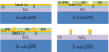
300nm Cu seed-layer was deposited by sputtering onto the 30 nm Ti adhesion-layer/300 nm SiO2/(100) Si-substrate. The wafer surface was coated with a photoresist from which solvent was removed by soft baking for 5 min. at 60°C. Using a photolithography process, the area of the vias and trenches for Cu RDL were exposed through the mask and then developed. Hard baking was performed for 20 min. at 120°C. Plasma descumming and H2SO4 cleaning was applied prior to diluted HF cleaning for 3 seconds and Cu electroplating as an RDL. The plating was carried out up to about 3 μm thickness using a forward and reverse current density of 0.64 mA/cm2. Resist removal was done using oxygen plasmas and then seed-layer was also etched in plasma etching equipment with a Ti adhesion-layer. The overall process flow for the realization of the Cu RDL is depicted in Figure 1.
2.2 Characterization of Cu RDL
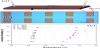
Electrical resistance measurements were made with a probe station and LCR meter (Agilent, Santa barbara, CA), as shown in Figure 2(a) to assess the resistance variation with time of the product Cu films. 9 points on the processed wafer were measured at each elapsed time. To complement the electrical measurement of Cu films, selective SIMS (CAMECA IMS 7f magnetic sector, Grésillons, France), X-ray photon spectroscopy (XPS) and X-ray induced Auger spectra (XAES) (PHI, VersaProbe XPS Microprobe, Chigasaki, Japan), X-ray diffraction (XRD) (Rigaku, Tokyo, Japan) experiments were performed with selected area of wafer where was close to electrical probing points. In these experiments, the impurities on and near the surface of the Cu RDL were detected by the SIMS operated at 6 kV and 10 nA for raster size of 175 μm x 175 μm with Cs+ source. The chemical states of the Cu RDL were characterized using XPS and XAES which were excited by monochromatic Al Kα radiation (1486.6 eV) with the X-ray power set at 4.5 W and the filament current of 20 μA. The base pressure in the analysis chamber was maintained lower than 1x10⁻¹⁰ Torr. The parameters for survey scans were : pass energy 58.7 eV; dwell time 50 ms; and energy step 0.5 eV in constant analyzer energy mode. High resolution X-ray photoelectron spectra were obtained at a pass energy of 20 eV, an energy step of 0.05 eV, and other parameters the same as for survey scans. XRD was used to assess the phases and crystallographic textures of the product films. Routine analysis was performed using a 2θ diffractometer with monochromatized Cu-K radiation that was supplied by a rotating anode generator operating at 30 kV and 50 mA with a scanning speed of 5°/min and a step size of 0.01°.
3. Results and Discussion
3.1 Electrical resistance evolution of Cu RDL
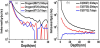
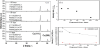
Figure 2(c) shows the electrical resistance evolution of Cu RDL films which were electroplated on the 300 nm seed Cu/30 nm adhesion Ti/300 nm SiO2/(100) Si-substrate. The electrical resistance of electroplated Cu films is evolved by slight increase until 7 days with a uniform distribution of electrical resistance, and then it increases very rapidly until 20 days with broader resistance distribution than that of the initial 7 days. It is distinctive that the increase in electrical resistance appears to be a linear function of √(elapsed time) within the initial 7 days as shown in Figure 3(a), meaning that the thickness of Cu RDL film decreases linearly with √(elapsed time) since the thickness t, of the rectangular block of uniform material with resistance R in Figure 2(a) and Figure 2(b) is given by [12]
t = (ρ/R)(L/W)
where ρ is the resistivity of Cu RDL film, and L and W represent the length and the width of Cu RDL block. Given the length L, the width W, and the resistivity of Cu RDL film ρ, one can extract the thickness of the layer of Cu RDL with √(exposed time) from the measured resistance with √(exposed time), as displayed in Figure 3(a). For long times at high-temperature conditions, oxide growth is proportional to the square root of time, and hence, the parabolic growth rate is frequently observed [13-15]. However, This is not the high temperature oxidation of Cu but the low temperature one. Therefore, the average resistance is not exactly proportional to the square root of exposed time until 7 days, as shown in Figure 3(a), while it is inversely satisfied with logarithmic exposed time, as represented by Figure 3(b). The copper oxide growth at low temperature is driven by an induced electric field, where the transport of Cu ions from the metal to the oxide-oxygen interface accelerates initial oxidation and rapidly attenuates with increasing oxide layer thickness, which is called ‘the inverse - logarithmic growth rate law [16]. Here, the Cu oxide thickness can be obtained by the following equation;
the Cu oxide thickness, d = initial Cu thickness at time zero – equation (1)
where initial Cu thickness was measured by the cross-sectional image taken right after pulling out the processed wafer from the electroplating bath, as shown in Figure 3(d). The inverse of the d is described as a function of logarithmic exposed time in Figure 3(c). However the resistance of Cu RDL made a jump to 3.8 Ω on average resistance at 20 days, indicating that the increase in electrical resistance is not controlled by the inverse - logarithmic growth rate law anymore, but by a new mechanism that will be described and supported by the SIMS depth profiles in Figure 4. In addition, the Cu RDL clearly shows electrical resistance variation, that was not severe within the initial 7 days but became severer as time goes on in the later 20 days. That has less spread range from 0.04 to 0.27 within the initial period of time and then more spread range 0.38 ~ 0.71, demonstrating that the obtained data are more variable as time continues.
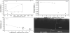
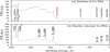
A SIMS was used to further evaluate the oxidation behavior on the surface of electroplated Cu RDL film in an air environment and impurity redistribution with time in electroplated Cu film, as shown in Fig. 4. Two elements were detected in the SIMS depth profiling. The oxidation behavior on the surface of RDL film was investigated through measuring the depth profiles of oxygen as a function of time, at 7, 20, and 33 days. Figure 4(a) shows oxygen piling up from the 10 nm depth of Cu RDL film to the surface during the initial 7 days, then it does not develop any changes further until 20 days, and then it broaden to the 30 nm depth until 33 days. It may be expected that oxygen piling up at 20 days is stronger in its intensity and thicker than that at 7 days because of the further oxidation of the electroplated Cu RDL. However, it shows almost the same oxygen profile as the data obtained at 7 days, implying that no further oxidation of Cu RDL has progressed any more since 7 days until 20 days. The answer to the question of resistance jump to 3.8 Ω at 20 days may be obtained from the measured depth profiles of Cl at different elapsed days, which yield information about the increase in electrical resistance not only without further oxidation since 7 days until 20 days, but also with oxidation during the initial oxidation for 7 days. It should be also noted that the depth profiles of Cl at 7 days is almost constant all through the measured thickness from the oxide/metal interface to ~70 nm depth. Therefore, oxygen is closely related to the oxide growth until 7 days on the surface while chlorine does the little oxidation since 7 days until 20 days inside the film. The last stage since 20 days until 33 days shows the difference in the depth profiles of oxygen and chlorine which is simultaneous piling up of oxygen and chlorine, leading to further increase in electrical resistance as shown in Figure 3(a) and Figure 2(c), with much broader resistance distribution than those at 7 days and 20 days as shown in Figure 2(c).
The oxide growth mechanism on the polycrystalline copper thin films, electroplated and exposed to ambient air conditions for long periods (on the order of a month) can be separated into different three stages of copper oxide growth: (a) Initial oxidation of a copper on the surface. The driving force for transport of Cu ions from the metal to the oxide/oxygen interface at low temperature is an electric field formed by positive ions of Cu at the metal/oxide interface and negative ions at the oxide/air interface. This is described by the following reaction [16-20]:
4Cu+(metal) + O2(gas) = 2Cu2O(solid)
As mentioned and presented in Figure 3 and Figure 4, the oxide layer grows depending initially on the concentration of the adsorbed oxygen on the surface until 4 days during which the induced electric field is strong enough to induce metal ions to migrate, so that it accelerates initial oxidation. As the oxide layer thickness increases, the induced electric field gets weak on and on, and the growth rate depends on the metal cation transport rate rather than the oxygen concentration in-between 4 days and 7 days. As can be seen in Figure 3(a) and Figure 3(b), concentration dependence deviates from the plot of resistance versus square root of elapsed time. Thus the oxide growth rate attenuates. This stage obeys the inverse - logarithmic growth rate law [16], as obtained from combining equation (1) and equation (2), and as shown in equation (4):
1/d = A – B ln (elapsed time)
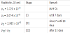
where A and B are fit parameters that contain information about the energy of Cu metal cation formation, the electric field, and the energy for diffusion across the oxide layer barrier. (b) Little oxidation and little moving of Cu metal ions toward the oxide/oxygen interface occur but the resistance of RDL layer increases due to moving of chlorine ions (Cl-) toward oxide/metal interface instead of moving of Cu metal ions toward the oxide/oxygen interface to form a copper (II) hydroxide Cu(OH)2 metastable phase as a wetting layer at the outer surface of the oxide layer, which was observed on the surface of polycrystalline Cu thin film evaporated thermally and exposed to ambient air conditions for long periods [21]. Simple calculations of the electrical resistivity (ρ) at different oxidation stages provide us with the information, summarized in Table 1, that the constant existence of chlorine ions in the film thickness increased the electrical resistivity to a value of 2.074 x 10⁻⁸ Ω cm at stage I and the moving of them toward the oxide/metal interface increased the resistivity to a higher value of 2.985 x 10⁻⁸ Ω cm at stage II. The result of stage II allows us to explain that the motion of charge carriers through the film lattice near the surface is affected more than any other depth by such a impurity that scatters charge carriers when they flow. This means further that charge carriers flows mainly near the surface because the flow path is the shortest way between two electrode on the film surface. The total resistivity at stage II is given by Mathiessen's rule [22], which states the resistivity of a material is the arithmetic sum of the individual contributions made by all sources of resistance
ρ(stage II) = ρ(temperature) + ρ(impurities) = ρ0(at 300 K) + ρI(Cl at stage I) + ρII(Cl at stage II) = 1.720 x 10⁻⁸ Ω·cm + 0.354 x 10⁻⁸ Ω·cm + 0.911 x 10⁻⁸ Ω·cm = 2.985 x 10⁻⁸ Ω·cm
The impurity, chlorine in the electroplated Cu thin film comes from copper electroplating solutions which contains Cu salt such as copper sulfate with Cu2+, acid like H2SO4, halide, e.g. Cl-, and organic additives. The use of organic additives and chloride ions in acid copper plating solution enables the void-free copper deposition. Chloride ions on their own act as the mild suppressor which slows down the deposition-rate of Cu on the wafer surface. What is not clear is that only Cl- moved to the oxide/metal interface without further involving of oxygen during stage II, which is compared with the 2nd stage oxidation of polycrystalline pure Cu thin film that forms a copper(II) hydroxide Cu(OH)2 metastable phase resulting from the interaction of Cu metal ions (Cu+) with hydroxyl (OH-) groups [21]. These differences in the 2nd stage oxidation do not lead to the formation of CuO layer during stage III, as will be presented by XPS results in Figure 5.
(c) Further oxidation of a copper native oxide, Cu2O layer occurs again while a continual moving of a chlorine ions (Cl-) toward oxide/ metal interface does simultaneously. Therefore, the resistance of RDL layer increases due to both continual moving of Cl- toward oxide/ metal interface and further oxidation of a copper on the surface again, resulting in higher piling of chlorine ions (Cl-) than that happened during the stage II and thus higher resistivity than any values obtained until the stage II, and thinner thickness of Cu RDL film, respectively. As shown in Table 1, the increase in the resistivity at stage III (ρIII) is believed to be caused by an additional contribution of impurity Cl- to the total resistivity at stage III and represented by ρIII > ρII because the two effects due to the increase in resistivity and the decrease in thickness are not separated independently. Moreover, the resistance of this stage III shows much broader distribution than those at 7 days and 20 days, as shown in Figure 2(c) and mentioned in the previous paragraph. Furthermore, it can be found in Figure 3(c) that the last data point at 129 days does not follow and deviate from the inverse - logarithmic growth rate law (dotted red arrows) to higher value of 1/d than that expected in the growth rate law as if the resistance of Cu RDL decreased, which brings about contradiction to the result of further piling of Cl obtained physically in SIMS at stage III and is aclue of explaining what is the driving force of the 3rd stage oxidation. The driving force for the 3rd stage oxidation is very questionable because the electric-field formed by Cu+ at the metal/oxide interface and negative ions at the oxide/air interface was not so strong enough that Cu+ could not migrate toward the oxide/oxygen interface and therefore Cu2O could not continue to grow. In addition, negative ions from the inside of Cu thin film have been already moved to the metal/ oxide interface in the stage II and they are still kept moving toward the metal/oxide interface. Nevertheless, the metal cations (Cu+) move toward the oxide/oxygen interface and interact with the adsorbed oxygen on the surface again in this stage III.
3.2 Physicochemical evolution of Cu RDL
SIMS depth profiles in Figure 4 demonstrate what is evolved in each stage, and where is the place each oxidation mechanism works. However, it is not able to explain what cause the RDL to reoxide in the stage III with the negative ions in the RDL film kept moving toward the oxide/metal interface like the stage II, as described in the previous section 3.1.
A more detailed investigation of the driving force at stage III induced or affected by any changes in the Cu2O/Cu thin film was performed via analysis of the time dependent microstructure evolution presented in Figure 6. The intensity from the Cu (111) plane and the Cu (200) plane decreases simultaneously but the intensity ratio of I(111)/I(200) holds constant as the exposed time elapses from 11 days to 31 days. However, the intensity ratio of I(111)/I(200) goes down even if the intensity from the electroplated Cu (111) plane keeps decreasing, but the intensity from the Cu (200) plane increases when the exposed time passes 58 days. A slight down of the intensity ratio happens further when it goes 102 days. The biggest change in the intensity ratio of I(111)/I(200) of the electroplated Cu thin film was observed when the exposed time was in-between 31 days and 58 days, which indicate that atoms in the Cu RDL thin film were rearranged at room temperature from an as-electroplated-Cu film, which is in general unstable because of high defect density until 31 days, into stable grains through formation of new grains with fewer defects at 58 days [23]. This is called 'recrystallization' that is generally a thermally activated process, however, it does not need any annealing for the electroplated Cu film. Therefore, it is expressed as a 'self-annealing' effect, which contains recrystallization and a consequent purification process during which the recrystallized grains grow larger by consuming defective grains, leaving defects mainly in the grain boundaries and film interface, so that the resistivity of the Cu RDL film also changes from high value of the as-electroplated film to low value of the recrystallized and purified films. The last data point deviated from the expected value on the graph in Figure 3(c) is more strongly affected by this 'self-annealing' effect than by the increase in the resistivity due to further piling up of Cl- and by the increase in the resistance due to further oxidation even thought these 3 phenomena happens simultaneously. Therefore, it should be noticed that ρIII can no longer be represented by ρIII > ρII because ρIII is given by:
ρIII = ρII + ρIII (Cl) - ρIII (self-annealing)
then becomes
= 2.985 x 10⁻⁸ Ω·cm + ρIII (Cl) - ρIII (self-annealing)
where absolute value of (ρIII (Cl)) < absolute value of (- ρIII (selfannealing)), resulting in ρIII < ρII. Based on the data point B and C in Figure 3(c), this is understood by the fact that the inverse of oxide thickness in stage III, C is almost the same as the previous one, B in stage II, indicating that the decrease in the film resistivity due to 'self-annealing' effect balances the increase in the film resistivity due to Cl piling and the reduction of RDL thickness due to oxidation.
These two points, B and C should not be plotted together on the same inverse - logarithmic growth rate law that initial oxidation in stage I occurred, otherwise the point B should be at point A because it was little oxidized even if it looks like an exact value on the graph following the inverse - logarithmic growth rate law. The reason why the point A is plotted at the point B is not due to the reduction of RDL thickness but due to the increase in resistivity of RDL, while point C should also be plotted at around point D if only the reduction of RDL thickness due to oxidation is correctly reflected on the graph except the 'self-annealing' effect and the increase in resistivity of RDL.
The 'self-annealing' causes another change in the mechanical properties of the as-plated Cu-films. From the XRD patterns in Figure 6(a), a ratio of relative peak intensities I(111)/I(200) of the electroplated Cu films was estimated as a function of exposed time. Although the ratio of intensities I(111)/I(200) is constant when it was measured at 11 days and 31 days, each I(111) or I(200) decreases with the exposed time; the relatively larger reduction in its intensity of I(111) than that of I(200) was observed, indicating that the (111) oriented grains are in a relatively higher energy state than the (200) oriented grains, and thus rearrangement of Cu atoms or short-range diffusion could occur to form a new set of defect-free grains. It is therefore possible that initial stage of recrystallization could occur in-between 20 days and 31 days; probably the very small grains are those that have recrystallized and (200) oriented. It was shown at 58 days that the ratio of I(111)/I(200) was decreased with the exposed time. The strong (111) texture becomes weaker than 31 days and the ratio of I(111)/I(200) is also changed into the lowest value of 2.7 by the relative increase in the intensity of (200) texture and by the relative decrease in the intensity of (111) texture. Moreover, the Cu RDL film is also contracted by defect reduction through 'recrystallization' and purification process. These however lead to the higher stress level of the oxide film formed on the surface of RDL Cu film than that of the oxide film before transition of RDL Cu film from strong (111) texture to relatively developed (200) texture. The in-plane lattice parameter of RDL Cu film facing to Cu2O thin film becomes small on average and thus the degree of misfit between the metal RDL Cu and the Cu2O at the interface is greater than that measured at 11 days and 31 days. As provided in Figure 6(b), a continual decrease in the intensity of (111) oriented grains was detected at all the exposed time, while the reverse intensity of (200) oriented grains to the increased one was obtained at 58 days and ever after, demonstrating that newly born grains could be (200) oriented and they grow consuming (111) oriented grains and therefore highly strained (111) grains are partially replaced by recrystallized (200) ones. These may be followed by grain growth and thus a continual increase in the intensity of (200) was detected by XRD at 102 days. Considering that the ratio I(111)/I(200) for randomly oriented Cu powder is equal to 2.17 [24], the ratio I(111)/I(200) of the RDL Cu films transits from relatively strong 3.7 into 2.7 through 'self-annealing'. The oxide layer over the self-annealed RDL Cu film is more strained and thus the unit cell of it will be more distorted [16, 25]. Cu2O film and metal Cu are both cubic systems [24]. Therefore the unit cell of the oxide is distorted into a tetragonal cell. Under this highly strained conditions the oxide layer may not strained by taking a structure where the oxide film and substrate metal retain their bulk lattice constant. Then the oxide and metal have the mismatch which is taken up by defects, called misfit dislocation [25].
The discussion of the previous section shows that a stable oxide film grows until it reaches a limiting thickness and then stops, as explained theoretically and experimentally [16]. The 3rd stage evolution in electrical and mechanical point of view stems from the recrystallization of the electroplated RDL Cu film, however, it is not clearly demonstrated what induce the stopped oxide growth to regrow further at stage III, but it should be underlined that this regrowth at stage III necessarily require the Cu+ moving again to the oxide/air interface, or O2- moving down to the oxide/metal interface. To describe the regrowth of the Cu2O layer at this stage III, interaction between atomic and electronic defects should be understood since the Cu2O layer is an ionic bond material in which negative ions balance positive ions, and therefore charge neutrality is satisfied [26]. From the results that chlorine is accumulated at the RDL Cu/oxide interface at stage II, and that the recrystallization of the RDL Cu layer leaves further piling of impurity chlorine at the RDL Cu/oxide interface at stage III, it is logically thought that the chlorine diffuses into Cu2O layer due to concentration gradient of the impurity chlorine and becomes an acceptor impurity in the Cu2O layer. The Cu2O layer is known as a p-type semiconductor [27,28] and can have the solubility of a solute, the impurity chlorine. Following Reiss [29], we may write the reaction
Cl = Cl- + e+
where e+ is a hole. Chlorine dissolves in the Cu2O layer and ionized until equilibrium is reached for this reaction, resulting in the increase in the concentration of holes from the acceptor. This drives a reaction of recombinating the increased holes and the equilibrium electrons in the Cu2O layer, tending to exhaust the concentration of electrons. Correspondingly, more metal will dissolve in the Cu2O layer and ionize from a reservoir which is in contact with the Cu2O layer, RDL Cu layer to maintain the electronic concentration, thereby, increasing the amount of dissolved copper in the Cu2O layer since Cu could be a donor impurity through the reaction
Cu = Cu2+ + 2e-
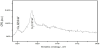
XPS was used to further evaluate the surface chemistry and the binding energy of the oxide formed on the Cu RDL films, to confirm that the formed oxide was only Cu2O, and therefore to confirm our assessment that the Cu2O growth continued to grow at stage III upon further moving of the Cu+ again to the oxide/air interface that was induced by Cl diffusion from the RDL film/oxide interface into the Cu2O, thereby, the increase in hole concentration in a p-type semiconductor, which require balancing of hole and electron concentration in the Cu2O film, therefore solving Cu atoms into the Cu2O film with electrons supplied. 270 μm x 70 μm area was investigated thoroughly using a survey scan. Figure 6 shows representative XPS survey spectra of a electroplated RDL Cu thin films that were exposed to ambient air for 140 days. The XPS survey spectrum Figure 5(a) occurring on the surface is almost the same as that occurring underneath, except carbon contamination at 285 eV and oxygen detection at 532.8 eV on the sample surface. More intense core-level lines of Cu, shown as a Cu2p doublet (Cu2p1/2 and Cu2p3/2) at 953 and at 932 eV, and clearer Auger Cu LMM triplet observed between 567 and 750 eV, are present in the sputter-cleaned Cu profile (Fig. 6(b)) with Cu3s at 123 eV, Cu3p at 77 eV, and Cu3d at 10 eV. The copper (I) oxide layer, Cu2O cannot be precisely characterized from the Cu2p spectrum due to a very small chemical shift of the Cu2p peak between metallic Cu and Cu2O oxide layer [30]. Therefore, a more detailed investigation of the signals from Cu2O and Cu was performed via analysis of the XAES of a Cu LMM transition, as shown in Figure 7. XAES spectra associated with CuO and Cu(OH)2 were not detected in the XAES spectra of any of the film investigated. Based on the data of Ilia Platzman et al. [21], the Cu(OH)2 film was formed on the Cu2O layer at stage II, and thus CuO was obtained from the transformation of a Cu(OH)2 metastable phase at stage III. This difference in the final phase reflects difference in the oxidation mechanism and driving force during the stage II and stage III. The last two stages of the overall Cu thin film oxidation mechanism explain the reason for the only and further formation of the Cu2O layer in the current work, which is compared to previous work mentioned earlier [16-21]. In any previous results, impurities in the polycrystalline Cu thin film and recrystallization of the polycrystalline Cu thin film during the proceeding of the Cu thin film oxidation have not been addressed on the effects of them on the oxidation mechanism and electrical resistance evolution of the Cu thin film. Moreover, the effects of the impurity and recrystallization of the polycrystalline Cu thin film begins after reaching a limiting thickness of a stable Cu2O growth at the end of stage I, so that we could obtain clearer results from the separate stages in time evolution of the oxidation mechanism without any simultaneous proceeding of oxidation.
4. Conclusion
Copper redistribution film was electroplated on a prepared and patterned Si interposer, and its electrical resistance and microstructural evolution was characterized using TEM, LCR meter, SIMS, XRD, XPS and XAES to give a clear explanation of the effects of impurity chlorine in the electroplated Cu RDL film on the surface reaction of oxygen in air at room temperature with Cu RDL film and on the resultant electrical resistance and microstructural evolution. The slight increase of electrical resistance was measured until 7 days when the growth of Cu2O layer on Cu RDL followed an inverse-logarithmic growth rate law due to the reaction of ourward Cu+ diffusion and negative O2- at low-temperature conditions in air, which is a well-known oxidation mechanism, resulting in reaching a limiting thickness of a stable Cu2O growth of stage I. After 20 days, contradictory increase in electrical resistance to the 'self annealing' of electroplated copper films at room temperature was induced by the chlorine impurity redistribution in Cu RDL or chlorine ions moving toward oxide/metal interface due to charge neutrality, resulting in scattering charge carriers near the Cu RDL surface when they flow. It is believed to be little oxidized at this stage II. Further oxidation was caused by the recrystallization of electroplated RDL Cu film from unstable state due to high defect density until 31 days into stable new (200) grains with fewer defects in-between 31~58 days, leaving defects mainly in the grain boundaries and at metal/oxide interface where chlorine impurity kept increasing its concentration. Thus it diffused into Cu2O layer with holes supplied, leading to electron supply in Cu2O layer for equilibrium concentration of electron-hole through solving metal Cu from the interface into Cu2O layer. Therefore the solved Cu+ could meet O2- at oxide/air interface, leading to reoxidation at stage III. The electrical resistance of Cu RDL film was dependent on the degree of recrystallization and simultaneously the impurity concentration at the metal/oxide interface. The former decreases while the latter increase resistivity of Cu RDL film. It is believed that further microstructural evolution comes from grain growth of the recrystallized (200) grains of Cu RDL film after 58 days until 102 days. Thus the same copper (I) oxide, Cu2O at stage III as at stage I can be grown on the outer surface of the previous Cu2O layer with the different driving force of electronic concentration difference at stage III from the electric field at stage I. The present approach gives a productive and helpful route to the 3-D integration of many chips on a Si interposer that becomes more and more applicable to various products.
Competing Interests
The authors have no competing interests with the work presented in this manuscript.
Author Contributions
All the authors substantially contributed to the study conception and design as well as the acquisition and interpretation of the data and drafting the manuscript.