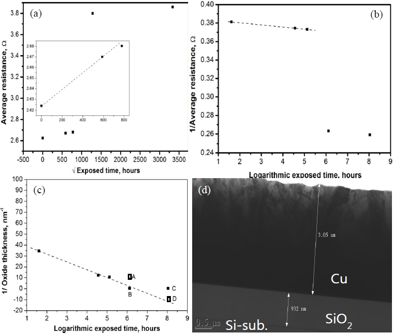
Figure 3: Evolution of Cu RDL films: (a) electrical resistance as a function of square root of exposed time to ambient air, (b) the inverse of average resistance as a function of logarithmic exposed time to ambient air, (c) the inverse of copper oxide thickness as a function of logarithmic exposed time to ambient air, (d) cross sectional TEM micrograph of a electroplated copper thin film. Note that the inset shows a deviated point at 7 days from the parabolic growth rate in Figure 3(a). The rectangles A and D in Figure 3(c) indicate assistant data to describe point B and C more easily.