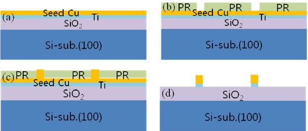
Figure 1: Schematic representation of the overall process flow for the RDL: (a) sputtering of 300 nm seed Cu/30 nm adhesion Ti/300 nm SiO2/(100) Si-substrate, (b) coating and soft baking of photo resist, exposing and developing of the vias and trenches for the RDL, and baking for 20 min. at 120°C prior to plasma descumming, H2SO4 cleaning, and HF cleaning in a diluted solution for 3 seconds, (c) RDL Cu electroplating with current density of 0.64 mA/cm2, (d) Removal of resist using oxygen plasma and seed-layer etching in plasma etching equipment.