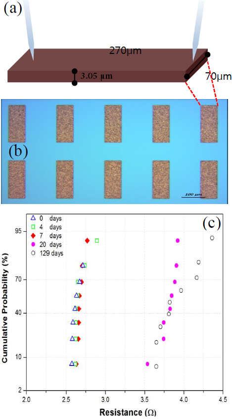
Figure 2: Experimental settings and electrical characterization of Cu RDL films electroplated on 300 nm seed Cu/30 nm adhesion Ti/300 nm SiO2/(100) Si-substrate: (a) schematic configuration of the electrical measurement; (b) an optical image of Cu RDL; (c) electrical resistance evolution of Cu RDL.