


1. Introduction
As a means for recovering a vast amount of waste heat, thermoelectric devices have been attracting a lot of interest. Although a wide variety of thermoelectric materials exist, candidates are still limited because of the strict demands for not only high thermoelectric performance but also nontoxicity, abundance, and inexpensiveness. The material thermoelectric performance is generally evaluated by a dimensionless figure of merit ZT, which is given by S2T/ρκ, where S is Seebeck coefficient, ρ is electrical resistivity, T is absolute temperature, and κ is thermal conductivity. As a potential material for satisfying the above demands with ZT over 1.0, higher manganese silicide (MnSi1.7), which is known to be semiconducting, has been focused on [1]. The crystal structure of MnSi1.7 is known as Nowotny chimney ladder phase, in which a manganese (Mn) sublattice forms a chimney like structure, while silicon (Si) exists in a helical fashion [2,3]. MnSi1.7 has an energy gap of 0.7-0.8 eV, and the large density of states near the Fermi energy contributes to large S [4,5]. The power factor (S2/ρ) exceeds 2×10⁻³ W/Km, while κ is low ranging from 2.0 to 3.0 W/Km owing to its complex crystal structure [2,3]. For further improvements in ZT, nanocomposite structures are known to be effective [6,7] and are relatively easy to be realized in thin films compared with bulk forms. In the author’s previous study, in which nanometer-scale MnSi1.7/Si multilayers were fabricated by controlled thermal diffusions of Mn and Si atoms, κ was successfully reduced to 1.0 W/Km, which is the experimentally observed minimum in MnSi1.7-related materials [8]. Recently, the importance of planar binary coupling reac-tions at the interface between transition metals and Si has been recognized for the formation of transition metal silicide thin films [9-11]. To modulate the texture and improve the thermoelectric properties of MnSi1.7- based com-posite thin films, planar Mn-Si coupling reactions should be investigated in detail and should be controlled.
In this study, we focused on planar Mn-Si coupling reactions and investigated changes of thermoelectric properties with the textures and crystal structures of MnSi1.7-based thin films. We fabricated MnSi1.7- based thin films by annealing multi-layered thin films in which Mn and Si layers were deposited alternately. To examine the nature of coupling reactions between Mn and Si in the post-annealing process, we first investigated dependence of crystal structures of annealed Mn/ Si bi-layered thin films and their thermoelectric properties on the composition ratio between Mn and Si. Next, we also evaluated the morphology of the fabricated MnSi1.7 thin film. After that, we tried to improve the morphology of MnSi1.7 thin films by reducing the initial thickness of Mn and Si layers since planar coupling reactions are considered to occur only in the vicinity of interfaces between Mn and Si layers. Then, for evaluating S of the thin films in high-temperature regions, we measured S of MnSi1.7 thin films on a thermally oxidized Si substrate and we clarified that the substrate is inappropriate for measuring S even if it is insulated with SiOx layers. Finally, we investigated an effect of post annealing on crystal structures and thermoelectric properties of MnSi1.7-based composite thin films with Si fabricated on sapphire substrates.
2. Experimental Procedure
Samples were prepared as follows. Multilayers (MLs) of Mn and Si were deposited by magnetron sputtering techniques with a base pressure of 10-6 Pa at room temperature (RT) on thermally oxidized Si substrates, in which the thickness of SiOx was 700 nm, and sapphire substrates. Hereafter, SiOx//, Sapp.//, and MLs (as-deposited) denote a thermally oxidized Si substrate, a sapphire substrate, and Mn/Si MLs that were not thermally annealed, respectively. The MLs (as-deposited) were deposited in the following order (from the substrate side): [Mn((100–t)/p)/Si(t/p)]p and [Mn(0.6×f)/Si(2.2×f)]48/f (thickness in nm). To change the Si/Mn composition ratio, the thickness of the Si layer, t, was varied from 50 to 100 nm. To modulate the texture of thin films, period p and thickness factor f were varied from 1 to 16 and from 1 to 6, respectively. The samples annealed at several temperatures between 0-800°C under vacuum of 10-6 Pa for 1 hour and in Ar-3% H2 atmosphere for 10 seconds to 1 hour.
The film composition was determined by inductively coupled plasma (ICP) mass spectrometry. The film structure was characterized by X-ray diffraction (XRD) using Cu Kα radiation (RINT1600, Rigaku Corp.), cross-sectional transmission electron microscopy (TEM) (JEMARM200F, JEOL Ltd.) with energy-dispersive X-ray spectroscopy (EDX) (HD-2700, Hitachi High-Technologies Corp.), and crosssectional scanning electron microscopy (SEM) (S-5200, Hitachi High-Technologies Corp.). The in-plane S and ρ were measured by 4- and 2-probe methods, respectively (ZEM-3, ADVANCE RIKO, Inc.).
3. Results and Discussion
3.1 Crystal structures and morphology of MnSi1.7 thin films fabricated from Mn/Si bi-layers
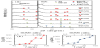
First, to examine the reaction between Mn and Si in the postannealing process, the dependence of fabricated materials and their thermoelectric properties on the Si/Mn composition ratio was investigated. Initial Mn/Si multilayers were deposited on Si/SiOx substrates, in a similar manner to that described in our previous report on MnSi1.7 thin films [8]. XRD profiles of a θ-2θ scan of SiOx// [Mn(100–t)/Si(t)]1 annealed at annealing temperature Ta of 800°C in a vacuum are shown in Figure 1 (a). The coexistence of Mn5Si3 and MnSi, that of MnSi and MnSi1.7, and that of MnSi1.7 and Si were observed when the Si layer thickness t was 50, 68, and 80 nm, respectively. The corresponding Si/Mn composition ratio determined by ICP is 0.6, 1.3, and 2.5, respectively. The sequence of material formation from Mn5Si3 to Si with increasing the Si/Mn composition ratio corresponds to the Si-Mn binary-phase diagram even when annealing temperature Ta was below the melting point of fabricated materials [12]. These results suggest that the observed manganese silicides were obtained by solidphase reactions, in this case, planar coupling reactions in the interface between Mn and Si layers as observed in previous reports on annealed Mn thin films on Si substrates [9,13]. Since the first nucleated phase in the interface between Mn and Si is known to be Mn5Si3 in planar Mn-Si coupling reactions following the rule proposed by Walser and Bené [14], the Ta of 800°C is enough high for consuming Mn and Si in the whole film through atomic diffusions. In fact, transition metals are known to be fast diffusers in Si at temperatures above 0.7 Tm (the melting point), in this case, 750-850°C [15]. On the other hand, Si single layer with t = 100 nm was not crystalized. This result indicates that planar binary coupling reactions support the crystallization of Si. Figure 1 (b) and (c) show dependence of S and ρ at room temperature on the Si layer thickness t, respectively. The corresponding Si/Mn composition ratio is also shown. Both S and ρ rapidly increased when Si/Mn composition ratio exceeded 1.7. This increase originates from formations of semiconducting MnSi1.7 and Si, while coexistence with metallic MnSi and/or Mn5Si3 is considered to keep the S low. As a result, the obtained S reached 300 μV/K when Si became the main phase with MnSi1.7 (t = 90 nm).
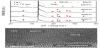
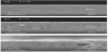
We next investigated the texture of MnSi1.7 thin films depending on the fabrication conditions. Figure 2 (a) shows XRD profiles of a θ-2θ scan of SiOx//[Mn(27)/Si(73)]1 annealed at 600-800°C under vacuum. The corresponding Si/Mn ratio of the films was confirmed to be about 1.7 by ICP. Single phase of MnSi1.7 was obtained when Ta was above 650°C, while MnSi instead of MnSi1.7 was observed when Ta was above 600°C. The cross-sectional TEM image in Figure 2 (b) shows the existence of large crystallized grains of MnSi1.7 phase, which was identified by EDX analysis, in SiOx//[Mn(27)/Si(73)]1 annealed at 800°C. As already noted, the first nucleated phase in planar Mn-Si coupling reactions should be Mn5Si3 followed by two reactions involving Si-richer compounds: (Mn5Si3 + 2Si → 5MnSi) and (4MnSi + 3Si → Mn4Si7) in the Si rich region as predicted theoretically [14,16,17] and previously observed in annealed Mn thin films on Si substrates [9]. Hence, the observed MnSi phase in thin films annealed at 600°C is considered to be the precursor of MnSi1.7 in planar Mn-Si coupling reactions. An SEM image of thin films annealed at 600°C is shown in Figure 3 (a). As shown in this image, the thin film has voids only in the vicinity of the interface between the Mn and Si layers. The fact that both unreacted Mn and Si exist at the bottom and top of the thin film, respectively, indicates that Ta of 600°C was not enough for atomic diffusion in the whole area of the thin film. This limited atomic diffusion lead to the formation of not MnSi1.7, which was observed in thin films annealed at above 600°C, but MnSi, which should appear before MnSi1.7 formation in planar Mn-Si coupling reactions as depicted in the above reaction formula regarding the formation of manganese silicides.
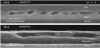
As for morphology, the thin film annealed at 600°C has even structures except for the interface between the Mn and Si layers. On the other hand, when Ta was increased to 800°C, the thin film has markedly depressed structures due to atomic diffusion across the whole thin-film area, as ob-served in Figure 3 (b). Defects and voids in this structure would degrade the material thermoelectric performance and cause difficulties in practical use.
3.2 Morphology improvements by thinning initial thickness of Mn and Si layers
To obtain smooth and voidless MnSi1.7 thin films, atomic diffusions of Mn and Si should be suppressed by controlling planar Mn-Si coupling reactions in the interfaces between the initial Mn and Si layers. Since the critical thickness for forming amorphous silicide to cause planar coupling reactions at the interface between transition metal and Si layers is known to be limited to about 2 nm [18], thinning of the initial Mn layers is considered to be effective for improving interfaces would suppress the large voids observed in thin films with a thick initial Mn layer formed by atomic diffusions since atomic diffusions would be prevented after the formation of manganese silicides. Figure 4 shows XRD profiles a θ-2θ scan of SiOx//[Mn(27/p)/Si(73/p)]p (p = 1, 4, 8, and 16) annealed at 800°C under vacuum for 1 hour. Diffraction peaks of MnSi1.7 are observed, and the peak structures for all films change little. In contrast to the crystal structure, the morphology of the thin films varies significantly depending on p, in other words, the initial thickness of the Mn and Si layers. Figure 5 shows cross-sectional SEM images of SiOx//[Mn(27/p)/Si(73/p)]p (p = 4, 8, and 16) annealed at 800°C under vacuum for 1 hour. The thin films have fewer voids and smooth structures with increasing p, compared with the thin film with p = 1 shown in Figure 3 (b). When the thickness of the Mn layer becomes less than 2 nm (p = 16), MnSi1.7 single phase with smooth void-free structures was formed. It is considered that this structure is obtained because planar Mn-Si coupling reactions occurred in the whole area of the thin films and diffusion of Mn atoms was limited by thinning the constituent layers.
3.3 Substrate effect on evaluation of Seebeck coefficient
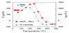
To evaluate the effect of kinds of substrate on S at high temperatures, S of MnSi1.7 thin films on Si/SiOx(700) substrates was measured. In particular, S of the fabricated smooth and homogeneous thin film with p = 16 was compared with that of a bare Si substrate, in which the SiOx layer on the substrate was removed by hydrofluoric acid. Figure 6 shows temperature dependence of S of SiOx//[Mn(27/16)/ Si(73/16)]16 annealed at 800°C under vacuum for 1 hour together with that of the bare Si substrate. S of MnSi1.7 thin films on Si/SiOx(700) substrate is almost same as that of MnSi1.7 bulk at room temperature. However, it can been seen from the figure that S of MnSi1.7 thin films rapidly increased at around 300°C followed by the sign inversion at around 350°C. In contrast, S of MnSi1.7 bulk is known to gradually increase with temperature and have a broad maximum at around 400- 500°C [2,3]. This anomalous temperature de-pendence resembles that of the bare Si substrate as shown in Figure 6. Hence, we suspect that this anomalous temperature dependence is not intrinsic: instead, it reflects the thermoelectric properties of not only the thin films on the substrate but also Si substrate itself which has large S. Similar anomalous temperature dependence in the case of MnSi1.7 thin films on a Si/SiOx(450) substrate has been previously reported [22]. According to the above results regarding S at high temperatures, the thickness of insulating SiOx layer, 700 nm, is considered to be not enough for evaluating thermoelectric properties especially at high temperatures. Accordingly, sapphire substrates, which are insulating, were used in our study for determining S at high temperatures. In the following sections, after investigating crystal structures of MnSi1.7- based composite thin films with Si on sapphire substrates, S and ρ of MnSi1.7 thin films were evaluated.
3.4 Crystal structures and thermoelectric properties of MnSi1.7-based composite thin films on sapphire substrate
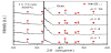
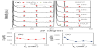
The crystal structures and thermoelectric properties of MnSi1.7- based thin films fabricated on sapphire substrates were investigated as follows. First, we investigated the effect of reducing the initial Mn layer thickness on the crystal structure and also on both S and ρ when the Si/Mn composition ratio exceeded 1.7 and the substrate was sapphire. Figure 7 (a) shows a dependence of XRD profiles of a θ-2θ scan on the thickness factor f in Sapp.//[Mn(0.7×f)/Si(2.2×f)]48/f annealed at 800°C under vacuum for 1 hour. The Si/Mn composition ratio is 2.1 and hence the coexistence of MnSi1.7 and Si is expected if all Mn react with Si. In all films, dif-fraction peaks from MnSi1.7 were observed and MnSi1.7 was found to be the main phase. On the other hand, the broad diffraction peaks of Si, which were observed when f is 4 or 6, disappear with decreasing f. In the case of f = 1, the peaks became sharp and large, indicating the MnSi1.7 grain growth and improved MnSi1.7 crystallinity. These results indicate that crystallized MnSi1.7-based composite thin films could be obtained by reducing the initial Mn layer thickness on the sapphire substrates. Figure 7 (b) and (c) show dependence of S and ρ at room temperature on thickness factor f, respectively. The ρ is about 30% small when f = 1 compared to the other films, while S stayed almost constant. This small ρ is considered to originate from suppression of grain boundary scatterings owing to the MnSi1.7 grain growth as was pointed out above. The improved crystallinity of MnSi1.7 as a result of planar Mn-Si coupling reactions occurring across the whole area of the thin films might also contribute. The ρ also gradually increases with f increase from 2 to 6. This increase may be due to the appearance of voids with increasing f as was observed in Figure 5. In fact, the density gradually decreases from 4.2 to 3.9 g/cm3 with f, while that hardly differs if compared between thin films with f = 1 and 2 (data are not shown here) [23]. The increase may also reflect suppression of point scatterings due to the shrink in size of remaining Si and/or the fraction decrease of Si resulting from the promotion of coupling reac reactions by thinning the initial Mn layer thickness.
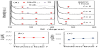
To investigate planar Mn-Si coupling reactions promoting the fabrication of our MnSi1.7-based thin films in detail, effects of annealing conditions on crystal structures and thermoelectric properties of fabricated MnSi1.7-based thin films were evaluated. Figure 8 (a) shows a dependence of XRD profiles of a θ-2θ scan on Ta for Sapp.//[Mn(0.7)/Si(2.2)]48 annealed at 200-800°C under vacuum. The XRD profiles are almost similar and, in the case that Ta was above 400°C, only diffraction peaks from MnSi1.7 are observed, while Mn/Si MLs (as-deposited) show no diffraction peak and the diffraction peak from MnSi appears in the case that Ta was 200°C. The amorphous state of Mn/Si MLs (as-deposited) agreed well with previous reports and indicates that planar Mn-Si coupling reactions contribute to the formation of MnSi1.7 [9]. The appearance of MnSi phase in thin films annealed at low Ta of 200°C may be due to insufficient reactions as was observed in Figure 3 (a). Figure 8 (b) and (c) show dependences of S and ρ at room temperature on Ta, respectively. Mn/Si MLs (asdeposited) shows S of 15 μV/K and ρ of 10 μΩm. Both the low S and ρ suggest that the Mn/Si MLs (as-deposited) are metallic and semiconducting MnSi1.7 was not formed. After Mn/Si MLs (asdeposited) were annealed at 200°C, both S and ρ increased above 150 μV/K and 250 μΩm, respectively, because of the formation of MnSi1.7 phase. The increase of ρ with increasing Ta may reflect that the fraction of semiconducting MnSi1.7 increases instead of the metallic secondary phase: MnSi and/or remaining Mn. On the other hand, the observed ρ is pretty high compared with that of bulk MnSi1.7, which ranges from 15 to 40 μΩm [2,3]. This large value is indicative of remnant of nearly insulating Si because the Si/Mn composition ratio of the film is 2.1 [24]. The ρ significantly decreased to 86 μΩm when Ta increased above 600°C. This reduction of ρ is possibly due to the promotion of the coupling reactions towards MnSi1.7 resulting in the decrease of the Si fraction. The improvements of crystallinity with increasing Ta and nano-crystallization of Si phase with increasing Ta might also contribute to the reduction of ρ. As discussed in the previous section for SiOx//[Mn(27)/Si(73)]1 annealed at 600°C, an inhomogeneous state was easily formed by insufficient atomic diffusions of Mn and Si in the thin films annealed at low Ta.
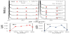
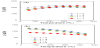
Note that MnSi1.7 phase was obtained even when Ta was 200°C, which is fairly low compared with other previous reports on MnSi1.7 -based thin films and bulk [2,3,9]. Absence of Mn5Si3, which is known to appear as a first phase through planar Mn-Si coupling reactions in Si-rich thin films [14,16,17], indicate that the effective Si concentration increased in the area where planar Mn-Si coupling reactions occurred due to the thinned initial Mn layers. According to the “effective heat of formation model” (EHF) [25], the heat of formation is given by the ratio between the effective concentration limiting element and the compound concentration-limiting element. By reducing the initial Mn layer thickness, it is possible to increase the effective Si concentration through the formation of intermixing interfaces (as discussed in the previous section). When effective Si concentration in the interfaces increased, MnSi1.7 becomes preferably stable in accord with the effective heat of formation diagram for Mn-Si shown in a previous report using EHF [26]. Figure 9 (a) shows a dependence of XRD profiles of a θ-2θ scan on the annealing time ta for Sapp.// [Mn(0.7)/Si(2.2)]48 annealed at 800°C in atmos-phere of Ar + 3% H2. In the case of all films, diffraction peaks from MnSi1.7 were observed and MnSi1.7 was found to be the main phase. Since the atomic diffusion strongly depends on both Ta and ta [15], MnSi should preferably appear when Ta and ta were decreased, as observed for SiOx//[Mn(27)/ Si(73)]1 annealed at 600°C. MnSi phase was observed only in thin films annealed for 1 hour and MnSi1.7 without coexistence of MnSi even for a short annealing time process also suggests that MnSi1.7 becomes energetically stable during silicide formation owing to the thinning of the initial layers. Figure 9 (b) and (c) show dependence of S and ρ at room temperature on ta, respectively. Clearly, ρ decreased rapidly with increasing ta and became almost constant when ta was longer than 1 minute, while S did not change much even when ta was increased. The decrease of ρ may be due to the homogenization of the fabricated MnSi1.7 phase driven by atomic diffusion through the an-nealing process. The nano-crystallization of Si, which could not be identified in this study, caused by annealing from amorphous phase in Mn/Si MLs (as-deposited) might also contribute to the decrease of ρ. Note that the ρ of thin films annealed for 1 hour in atmosphere of Ar + 3% H2 is about half of that of thin films annealed for 1 hour in a vacuum. The appearance of MnSi phase, which was not observed in thin films annealed in a vacuum, suggest that Mn reacts with Si insufficiently and resultantly metallic MnSi makes the ρ low compared with thin films annealed in a vacuum.
Finally, we evaluated S and ρ of fabricated MnSi1.7 thin films at high temperatures because MnSi1.7 is known to show the maximum power factor, S2/ρ, at around 400-500°C [2,3]. Figure 10 (a) and (b) show dependence of S and ρ on temperature for Sapp.//[Mn(0.7)/Si(2.2)]48 annealed at 800°C for 1 hour under vacuum, respectively. Temperature was varied from 50 to 450°C. Annealing temperature Ta and annealing time ta were fixed to 800°C and 1 hour, respectively, because, according to the results in the previous sections, high Ta and long ta were found to be effective for increasing the power factor. S slightly increased with temperature and reached a maximum around 400°C. Note that this behavior is almost consistent with previous reports on MnSi1.7 bulk [2,3] and clearly different from that of thin films on the Si/SiOx(700) substrates. The difference in S behavior depending on substrates indicates that, for evaluating S and ρ, the insulating substrates should be carefully chosen. Moreover, S reached 225 μV/K at 390°C, which is close to the maximum value of MnSi1.7-based compounds. On the other hand, ρ decreased with increasing temperature. Since MnSi1.7 is a degenerate semiconductor, ρ was reported to increase with increasing temperature and show a maximum at around 400-500°C [2,3]. This difference from the reported behaviors in temperature dependence may originate from the residual Si in the composite films because the Si/Mn composition ratio of the fabricated thin films is 2.1. Similar temperature dependence of ρ in the case of Si-rich MnSi1.7 thin films has been also previously reported [27]. As for f dependence, S of thin films with f = 1 had stronger temperature dependence than those with f = 2, 4, and 6, while ρ of the thin film with f = 1 was much lower than those with f = 2, 4, and 6. The behavior of S may reflect the improved crystallinity of semiconducting MnSi1.7 with decreasing the initial thickness of the Mn layers (as discussed in the previous section). The reduction of ρ with decreasing f is considered to be due to the suppression of grain boundary scatterings, disappearance of voids, and the suppression of point scatterings of remaining Si as was discussed previously.
4. Conclusion
Thermoelectric properties of MnSi1.7-based composite thin films with Si were investigated when the texture of thin films was changed. MnSi1.7 thin films were fabricated by annealing Mn/Si multilayered thin films and initial thickness of the constituent layers was changed to modulate the texture. By thinning the initial constituent layers, smooth and voidless crystalline MnSi1.7-based thin films were obtained because planar Mn-Si coupling reactions are considered to occur across the whole area of the thin films. It was found that MnSi1.7 may be the first formed phase by planar Mn-Si coupling reactions in thin films with the initial Mn layer thickness below 2 nm. The effect of annealing temperature and annealing time on crystal structure and thermoelectric properties was also investigated. As a result, ρ was decreased about 30% by reducing initial Mn thickness and large S of 225 μV/K was obtained at 390°C.
Competing Interests
The authors declare that they have no competing interests.
Author Contributions
All the authors substantially contributed to the study conception, the acquisition of results, and the interpretations as well as drafting the manuscript.
Acknowledgments
This paper is based on results obtained from the Future Pioneering Program “Research and Development of Thermal Management and Technology” commissioned by the New Energy and Industrial Technology Development Organization (NEDO).