Profile
International Journal of Metallurgical & Materials Engineering Volume 3 (2017), Article ID 3:IJMME-138, 5 pages
http://dx.doi.org/10.15344/2455-2372/2017/138
Research Article
Novel Graphene-Silicon Heterostructure Device with a Gate-Controlled Schottky Barrier

Pengfei Zhang, Beibei Guo and Dongyun Wan*

School of Materials Science and Engineering, Shanghai University, Shanghai, China
Dr. Dongyun Wan, School of Materials Science and Engineering, Shanghai University, Shanghai 200444, China; E-mail: wandy@mail.sic.ac.cn
22 November 2017; 27 December 2017; 29 December 2017
Zhang P, Guo B, Wan D (2017) Reactive Oxygen Species in Novel Hydrometallurgical Processes. Int J Metall Mater Eng 3: 138. doi: https://doi.org/10.15344/2455-2372/2017/138
The work was supported by the jointed foundation from National Natural Science Foundation of China and the big science facility of Chinese Academy of Sciences (No. U1632108).

Abstract

Although the Graphene-Silicon (Gr-Si) based configurations have received extensive attention in electronics and optoelectronics, sufficient on/off current ratio Ion / Ioff and new applications are still limited by conventional device structures. In this study, we show a new structure of vertical ambipolar barristors based on silicon-graphene-h-BN-graphene sandwich structure, which can be effectively modulated by the gate voltage for that the graphene is ambipolar. The bottom graphene acts as a gate-tunable “active contact” and the top graphene is used as the gate electrode with the help of the hexagonal boron nitride (h-BN) as a transparent dielectric layer. Under the influence of the gate voltage, the Gr-Si configuration can be flexible modulated with an ON-OFF ratio exceeding 103. Besides, a normal photovoltaic properties of the devices has been characterized due to the application of its transparent two-dimensional materials. This unconventional Gr-Si configuration has a potential meaning for future electronics and optoelectronics based on graphene or other two-dimensional van der Waals heterostructures.


1. Introduction

Graphene, a single carbon atomic layer with a honeycomb structure, has received extensive attention due to its superior electrical, optical and mechanical properties [1-5]. The visible light transmittanceof graphene has been proved to be as high as 97.7% with a tiny conductivity of 30Ω/, which is much better than the widely used commercial transparent electrodes of indium doped tin oxide (ITO, typically 30-80Ω/ with a visible light transmittance of 90%) [6,7]. Besides, graphene is more readily scalable and has lower contact resistance. It thus has developed rapidly and is widely used as transparent electrodes for electronics and optoelectronics, including rectifier diodes, light emitting diodes (LED), photodetectors, solar cells and so on [8-14]. Among these research works, the combination of graphene and silicon for optoelectronics has potential significance considering that silicon is the main commercial material in semiconductor industry [15-17].

For the reason of the work function difference between graphene and silicon, the contact of the graphene and silicon results in charge transfer, yielding a built-in electric field on the interface. When the light irradiates on the device, sunlit silicon absorbs photons and generates electron-hole pairs. Thus, the photogenerated carriers are separated under the influence of the built-in electric field and respectively collected by graphene and silicon, resulting in the generation of photocurrent. Following this principle, the graphene-silicon (Gr-Si) configuration has made significant progress. Recently, the efficiency of the Gr-Si solar cells have been enhanced to 14.5% with the help of a colloidal antireflection coating and nitric acid doping graphene [18]. Besides, the Gr/Si configuration can also be used to develop highly sensitive photodetectors with a photovoltage responsivity exceeding 107 V/W [19]. However, thelack of bandgap causes that the electrical properties of graphene cannot be effectively regulated in the traditional device structure, which limits its wide application in electronic devices. Atoms doping is considered as an effective solution to the problem but at the expense of reducing physical properties. In further research works, graphene was proved to be ambipolar, meaning that the major charge-carrier type and density can be easily controlled by the electric field [20-26]. Based on this, exploiting graphene as a unique “active contact” with tunable work function should allow some flexible design of devices. This paper primarily focuses on a feasible way to construct tunable Optoelectronic devices based on an untraditional Gr-Si configuration.

In this work, a novel gate-controlled graphene/h-BN/graphene/ Si heterojunction was demonstrated. The device can be dynamically and flexibly modulated under the effect of the electric field, and tuned as modifiable device, which exhibit disparate electronic and photovoltaic properties. This unconventional device structure and ambipolar reconfigurable devices characteristics will further expand the new applications of graphene structure configuration, and open up potential opportunities for future electronic and optoelectronic devices [24,27-29].

2. Methods

2.1 Fabrication of graphene/h-BN/graphene/Si Heterostructure Devices

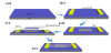
The schematic diagram of the device fabrication process is shown in Figure 1. Few-layer graphene flakes, h-BN were prepared using a mechanical exfoliation method from bulk crystals [30], and all the two-dimensional materials were transferred on a transparent polydimethylsiloxane (PDMS) film using a 3M Scotch tape. Besides, a kind of n-type silicon wafer covered with a 300-nm-thick thermal oxide (SiO2) film was used as substrate to complete the device structure. Firstly, electron-beam lithography (EBL) was used to define Au/Ni (50nm/5nm) electrodes on the cleaned wafer. A 15 um2 area silicon square window between the two electrodes was secondly etched using a buffered oxide etchant (BOE) etching method under the help of EBL. With the help of an optical microscope, a few-layer graphene flake was first exfoliated on the prepared substrate. After a slight press, the graphene was transferred to the desired position due to the affinity difference between the PDMS and Si. The h-BN was aligned on the obtained graphene/silicon heterostructure using a similar method, and the last piece of graphene followed. Thus the graphene/h-BN/graphene/silicon heterostructure was formed.

figure 1
Figure 1: Schematic diagram of the graphene/n-silicon device fabrication process. (a) The source material of silicon with 300-nm-thick thermal oxide film on one sides. (b) Electron-beam lithography (EBL) was used to define Au/Ni electrodes on the Si02 layer. (c) An area of 15 um2 SiO2 was totally etched by BOE between the two electrodes. (d) Three pieces of two-dimensional materials (graphene/h-BN/graphene) were transferred on the Si window in turn. The first graphene totally covers the exposed Si and contacts with one of the Au/Ni electrode, and h-BN follows. The second graphene covers the window and contacts with another electrode. (e) The final Gr/Si device obtained.

3. Characterization

Keithley 4200-SCS semiconductor analyzer was used to characterize the electrical properties of the devices in a probe station with a high vacuum of 10-4 Pa. Optoelectronic characteristics were measured with a laser of 638 nm in wavelength (LSR638CPD-1W, from Lasever Company, Ltd.).

4. Result and Discussion

The optical microscope image of a Gr/Si device is showed in Figure 2a, and Figure 2b correspondingly shows a sectional view of the window.

figure 2
Figure 2: (a) Optical micrograph of Gr-Si device. (b) Schematic diagram of the window.

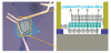
As we can see in the schematic diagram, the bottom graphene was in contact with the silicon to form the Gr/Si heterojunction conductive channel. The top graphene was used as the back electrode with the help of h-BN acting as a dielectric layer.

Figure 3a shows transfer characteristic curves of the Gr-Si FET with a bias voltage VDS of ±1 V, respectively. With the gate voltage Vgate increases from -5 v to +5 v, the forward current increases rapidly while the reverse current increases even more. The current and bias voltage characteristics of the Gr/Si device at various fixed Vgate values are shown in Figure 3b, which demonstrates that the rectification behavior of the heterostructure reduces slowly with the increase of Vgate. With the help of the top gate electrode and gate dielectric above the graphene, the Schottky barrier (SB) height changes, resulting in the change of the injection of the majority carriers from graphene to silicon. This electrical phenomenon corresponds to the reason that the top gate directly controls the magnitude of the current across the Gr/Si heterojunction with the help of its ambipolar characteristics.

figure 3
Figure 3: (a) Transfer characteristic curves of the Gr/n-Si heterojunction device (Gr as drain) with VDS of ±1 V. (b) The current and bias voltage characteristics of the Gr/Si heterojunction at various fixed Vgate values, Vgate varies in the range of -5 V to 5 V, with a step size of 1 V for each curve. The blue arrow indicates the direction of increasing Vgate. (c and d) Schematic band diagrams of the heterojunction with the electric field effect generated by the gate on the top of graphene. (c)Negative gate voltage. (d) Positive gate voltage.

The characteristic of the Gr/Si device can be expressed by the diode equation:

Ι=ΑΑ* T 2 exp( -qΦb KBT )[ exp( qVbias ηidKBT )1 ]

Where A is the area of the Schottky junction, A* is the effective Richardson constant, q is the elementary charge, kB is the Boltzmann constant, and T is the temperature. We analyze the electrical properties of the device in the reverse bias saturation regime [ exp( qVbias/ηidKBT )<<1 ] , resulting in that the diode current becomes insensitive to Vbias and Ι  T 2 exp( -qΦb KBT ) . The schematic band diagrams of the Gr/Si heterojunction on negative gate voltage (Figure 3c) and Positive gate voltage (Figure 3d) are used to analyze the internal charges change process. When the back voltage Vgate is on negative gate voltage, extra positive charges generate and the fermi level of graphene drops, leading to a higher barrier height. When Vgate is on positive gate voltage, extra negative charges generate and the majority carriers from graphene to silicon increase, which is the main reason of the phenomenon that the reverse current increases rapidly in reverse bias.

To further analyze the internal changes of the Gr-Si devices, we quantitatively calculate the barrier height of the Gr/Silicon heterojunction at different gate voltages. The forward current through a Schottky junction follows the thermionic emission model, which can be represented by [31]:

Ι=ΙS[ exp( eVD nKT )1 ]

Where Is is the reverse saturation current, e is the electronic charge, VD is the bias voltage across the Schottky junction, n is the ideality factor, k is the Boltzmann constant, T is the absolute temperature, and Rs is the series resistance. Besides, Is can also be represented by:

ΙS=Αeff Α Τ 2 exp( eΦΒ ΚΤ )

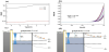
Where Aeff is the effective area of Schottky junction, A** is the Richardson constant, and ΦB is the Schottky barrier height. The two equations mentioned above can also determine the relationship between current, voltage and the barrier height of the Gr-Si heterostructure. By analyzing the dark-state voltage-current data in different gate voltage, the barrier height as a function of Vgate is shown in Figure 4a, which indicates that the ΦB decreases rapidly with the increase of Vgate.

figure 4
Figure 4: (a) The SB height as a function of Vgate. (b) Open-circuit voltage VOC as a function of the Vgate.

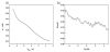
Figure 4b plots open circuit voltage Voc as a function of the gate voltage Vgate. The Voc is generally decreasing with the increasing Vgate in the range of -5 V - 5V, which is just corresponding to the analysis of the Schematic band diagram.

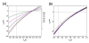
The development of Gr-Si heterostructures for semiconductor optoelectronic devices is of great significance. Considering that, we also characterized photovoltaic properties of the Gr-Si device in our experiments. Figure 5a shows Ids–Vds curves of the Gr–Si heterostructure under light illumination (a laser of 638 nm) with the gate fixed at 0. The results demonstrate that the Ids–Vds curve keeps on shifting upward with the laser power (Plaser ) increasing, which is operated as a typical diode and exhibits an obvious photovoltaic response. With a laser power of 627 nW, the generated open-circuit voltage (VOC) and short-circuit current (ISC) are 0.09 V and 50 nA, respectively. Figure 5b shows the Ids–Vds characteristic curves of the device under light illumination with different gate voltage, which indicates that the gate voltage had an obvious impact on the photovoltaic response of the Gr-Si device [32].

figure 5
Figure 5: (a) Ids–Vds characteristic curves of the device under light illumination with different powers (Vgate=0 V). (b) Ids–Vds characteristic curves of the device under light illumination with different gate. The blue arrow indicates the direction of increasing Vgate.

5. Conclusions

In conclusion, an outstanding vertical stacked optoelectronic device based on a graphene/h-BN/graphene/Si heterostructure has been realized and this gate-controlled device can be dynamically and flexibly modulated under the effect of the electric field with a high on/ off ratio of ~1.56x10³, which can be improved with well-developed semiconductor processes because there is not a fundamental (or structural) limit. The study should facilitate the development of the Gr-Si device and expand the applications of graphene and other twodimensional materials [33,34].

Competing Interests

The authors declare that they have no competing interests.


References

  1. Castro Neto AH, Guinea F, Peres NMR, Novoselov KS, Geim AK, et al. (2009) The electronic properties of graphene. Reviews of Modern. Physics 81: 109-162. View
  2. Nair RR, Blake P, Grigorenko AN, Novoselov KS, Booth TJ, et al. (2008) Fine structure constant defines visual transparency of graphene. Science 320: 1308. View
  3. Lee C, Wei X, Kysar JW, Hone J (2008) Measurement of the elastic properties and intrinsic strength of monolayer graphene. Science 321: 385- 388. View
  4. Geim AK, Novoselov KS (2007) The rise of graphene. Nature materials 6: 183-191. View
  5. Novoselov KS, Fal'ko VI, Colombo L, Gellert PR, Schwab MG, et al. (2012) A roadmap for graphene. Nature 490: 192-200. View
  6. Chen JH, Jang C, Xiao S, Ishigami M, Fuhrer MS, et al. (2008) Intrinsic and extrinsic performance limits of graphene devices on SiO2. Nature nanotechnology 3: 206-209. View
  7. Zhu Y, Sun Z, Yan Z, Jin Z, Tour JM, et al. (2011) Rational design of hybrid graphene films for high-performance transparent electrodes. ACS nano 5: 6472-6479. View
  8. Chang H, Wang G, Yang A, Tao X, Liu X, et al. (2010) A Transparent, Flexible, Low-Temperature, and Solution-Processible Graphene Composite Electrode. Advanced Functional Materials 20: 2893-2902. View
  9. Wassei JK, Kaner RB (2010) Graphene, a promising transparent conductor. Materials Today13: 52-59. View
  10. Kim KS, Zhao Y, Jang H, Lee SY, Kim JM, et al. (2009) Large-scale pattern growth of graphene films for stretchable transparent electrodes. Nature 457: 706-710. View
  11. Wang X, Zhi L, Müllen K (2008) Transparent, conductive graphene electrodes for dye-sensitized solar cells. Nano letters 8: 323-327. View
  12. Hsu CL, Lin CT, Huang JH, Chu CW, Wei KH, et al. (2012) Layer-by-layer graphene/TCNQ stacked films as conducting anodes for organic solar cells. ACS nano 6: 5031-5039. View
  13. Tung VC, Chen LM, Allen MJ, Wassei JK, Nelson K, et al. (2009) Lowtemperature solution processing of graphene-carbon nanotube hybrid materials for high-performance transparent conductors. Nano letters 9: 1949-1955. View
  14. Liu Z, Liu Q, Huang Y, Ma Y, Yin S, et al. (2008) Organic Photovoltaic Devices Based on a Novel Acceptor Material: Graphene. Advanced Materials 20: 3924-3930. View
  15. Chen CC, Aykol M, Chang CC, Levi AF, Cronin SB, et al. (2011) Graphenesilicon Schottky diodes. Nano letters 11: 1863-1867. View
  16. Feng T, Xie D, Lin Y, Zang Y, Ren T, et al. (2011) Graphene based Schottky junction solar cells on patterned silicon-pillar-array substrate. Applied Physics Letters 99: 233505. View
  17. Xie C, Lv P, Nie B, Jie J, Zhang X, et al. (2011) Monolayer graphene film/ silicon nanowire array Schottky junction solar cells. Applied Physics Letters 99: 133113. View
  18. Shi E, Li H, Yang L, Zhang L, Li Z, et al. (2013) Colloidal antireflection coating improves graphene-silicon solar cells. Nano letters 13: 1776-1781. View
  19. Zhou Y, Huang A, Li Y, Ji S, Gao Y, et al. (2013) Surface plasmon resonance induced excellent solar control for VO(2)@SiO(2) nanorodsbased thermochromic foils. Nanoscale 5: 9208-9213. View
  20. Gusynin VP, Sharapov SG, Carbotte JP (2007) Magneto-optical conductivity in graphene. Journal of Physics: Condensed Matter 19: 026222. View
  21. Yang X, Liu G, Rostami M, Balandin AA, Mohanram K, et al. (2011) Graphene Ambipolar Multiplier Phase Detector. IEEE Electron Device Letters 32: 1328-1330. View
  22. Tian JF, Jauregui LA, Lopez G, Cao H, Chen YP, et al. (2010) Ambipolar graphene field effect transistors by local metal side gates. Applied Physics Letters 96: 263110. View
  23. Herring PK, Hsu AL, Gabor NM, Shin YC, Kong J, et al. (2014) Photoresponse of an electrically tunable ambipolar graphene infrared thermocouple. Nano letters 14: 901-907. View
  24. Wang H, Hsu A, Wu J, Kong J, Palacios T, et al. (2010) Graphene-Based Ambipolar RF Mixers. IEEE Electron Device Letters 31: 906-908. View
  25. Xia F, Perebeinos V, Lin YM, Wu Y, Avouris P, et al. (2011) The origins and limits of metal-graphene junction resistance. Nature nanotechnology 6: 179-184. View
  26. Yu YJ, Zhao Y, Ryu S, Brus LE, Kim KS, et al. (2009) Tuning the graphene work function by electric field effect. Nano letters 9: 3430-3434. View
  27. Han W, Nezich D, Jing K, Palacios T (2009) Graphene Frequency Multipliers. IEEE Electron Device Letters 30: 547-549. View
  28. Myung S, Park J, Lee H, Kim KS, Hong S, et al. (2010) Ambipolar memory devices based on reduced graphene oxide and nanoparticles. Adv Mater 22: 2045-2049. View
  29. Lemme MC, Echtermeyer TJ, Baus M, Kurz HA (2007) Graphene Field- Effect Device. IEEE Electron Device Letters 28: 282-284. View
  30. Martinez A, Fuse K, Yamashita S (2011) Mechanical exfoliation of graphene for the passive mode-locking of fiber lasers. Applied Physics Letters 99: 121107. View
  31. Wang X, Li D, Zhang Q, Zou L, Wang F, et al. (2015) Study on the graphene/ silicon Schottky diodes by transferring graphene transparent electrodes on silicon. Thin Solid Films 592: 281-286. View
  32. An X, Liu F, Jung YJ, Kar S (2013) Tunable graphene-silicon heterojunctions for ultrasensitive photodetection. Nano letters 13: 909-916. View
  33. Butler SZ, Hollen SM, Cao L, Cui Y, Gupta JA, et al. (2013) Progress, challenges, and opportunities in two-dimensional materials beyond graphene. ACS nano 7: 2898-2926. View
  34. Xu M, Liang T, Shi M, Chen H (2013) Graphene-like two-dimensional materials. Chemical reviews 113: 3766-3798. View