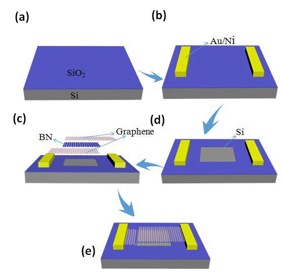
Figure 1: Schematic diagram of the graphene/n-silicon device fabrication process. (a) The source material of silicon with 300-nm-thick thermal oxide film on one sides. (b) Electron-beam lithography (EBL) was used to define Au/Ni electrodes on the Si02 layer. (c) An area of 15 um2 SiO2 was totally etched by BOE between the two electrodes. (d) Three pieces of two-dimensional materials (graphene/h-BN/graphene) were transferred on the Si window in turn. The first graphene totally covers the exposed Si and contacts with one of the Au/Ni electrode, and h-BN follows. The second graphene covers the window and contacts with another electrode. (e) The final Gr/Si device obtained.