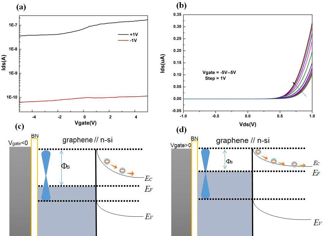
Figure 3: (a) Transfer characteristic curves of the Gr/n-Si heterojunction device (Gr as drain) with VDS of ±1 V. (b) The current and bias voltage characteristics of the Gr/Si heterojunction at various fixed Vgate values, Vgate varies in the range of -5 V to 5 V, with a step size of 1 V for each curve. The blue arrow indicates the direction of increasing Vgate. (c and d) Schematic band diagrams of the heterojunction with the electric field effect generated by the gate on the top of graphene. (c)Negative gate voltage. (d) Positive gate voltage.