


1. Introduction
Organic thin-film transistors (TFTs) are attracting much interest because of their simple and low-temperature process ability. It is envisaged that they will have enormous market in a wide range of applications, for example as the driving elements for flexible displays, radio-frequency identification tags and large area sensors [1-3]. Previous investigations on organic TFTs have focused on materials [4], interfacial properties [5], source/drain contact engineering [6] and processing techniques [7], to enhance the TFT performance. Among the characteristic parameters, the field-effect mobility is known to be greatly influenced by the deposition conditions and consequent crystallinity of organic semiconductors. Likewise, the chemical and morphological properties of a gate insulator are deemed decisive to the field-effect mobility in bottom-gate organic TFTs by influencing the crystalline growth of an organic semiconductor. Several works have shown that the rough surface of a gate insulator causes a reduction in the field-effect mobility [5,8]. In contrast, recent studies reported that the crystalline growth of organic semiconductors and the performance of organic TFTs can be improved by introducing structured morphologies on the surface of a gate insulator [9,10], which motivates our research into cowl-shaped nanostructures for application in organic TFTs.
In this study, we show that hydrophobic nanostructures with a cowl shape facilitate the upright growth of pentacene molecules to the substrate. The influence of hydrophobic cowl-shaped nanostructures on the morphological and structural characteristics of pentacene films are investigated. The enhancement in the field-effect mobility of pentacene-based TFTs fabricated with these nanostructures is reported.
2. Experimental Procedure
To fabricate pentacene TFTs, a 150-nm-thick Al gate was deposited on a glass substrate using the first shadow mask. Poly (4-vinylphenol) (PVP) with a cross-linking agent was spin-coated on the gate-patterned substrates and baked consecutively at 175°C for 1 h in a vacuum oven. A 480-nm-thick layer of cross-linked PVP (cPVP) was used as a gate insulator. For the formation of cowl-shaped nanostructures, the polyurethane-based solution was spin-coated onto the cPVP-coated substrate, followed by thermal curing at 100°C for 1h. Pentacene (TCI, used without further purification) was thermally evaporated through the second shadow mask onto the insulator-coated substrates at a rate of 0.05 nm/s, up to a thickness of 90 nm. Top-contact/bottom-gate organic TFTs were constructed by depositing 50-nm-thick Au source/ drain electrodes using the third mask. The channel length (L) and width (W) of our TFT were 50 and 300 μm, respectively.
The surface energy and morphologies of insulator films were evaluated by the contact angle measured using a contact angle meter GSA10 (KRUSS Co., Ltd.) and by atomic force microscopy (AFM) (XE150, PSIA Inc.), respectively. The morphological and structural characteristics of pentacene films were performed by AFM and X-ray diffraction (XRD) (DMAX 2500, Rigaku Co.), respectively. The electrical characteristics of the pentacene TFTs were measured with a semiconductor analyzer (EL 421C, Elecs Co.).
3. Results and Discussion
Figure 1a shows the AFM image of the cPVP film containing cowlshaped nanostructures. While the bare cPVP surface was very smooth with a root-mean-square (RMS) surface roughness of 0.1 nm (Figure 1a, inset), cowl-shaped nanostructures resulted in a rough surface (RMS surface roughness, 21.2 nm); the diameter and height of cowlshaped nanostructures were up to 15 and 40 nm, respectively. The surface energies of the bare cPVP and the nanostructured cPVP films were investigated using distilled-water contact angle measurement. The direct measurement of contact angle from sessile drop is used and the angle is measured by aligning a tangent with the drop profile at the point of contact with the solid surface. Figure 1b shows that water is wetting the bare cPVP film with a contact angle of about 59°, while almost non-wetting on the nanostructured cPVP film with a contact angle of about 107° as shown in Figure 1b. The surface free energy (Υp ) for both films was evaluated using the measured contact angles ( θ0),
Where Υw is the water surface free energy (73 mJ/m2) [11]. The Υp's of the bare cPVP and the nanostructured cPVP films are calculated to be about 41.9 and 9.1 mJ/m2, respectively. The hydrophobic feature of the nanostructured cPVP film is intrinsically related with the hydrophobicity of polyurethane, which is generally used in waterproof stuffs. Note that hydrophilic liquids poorly wet hydrophobic surfaces owing to large energy difference, and vice versa. In the case of the nanostructured cPVP layer, hydrophobic polyurethane molecules would prefer aggregating to completely spreading over the relatively hydrophilic cPVP surface in order to lower its surface energy. Hence, we can attribute the origin of rough surface with cowl-shaped nanostructures of the nanostructured cPVP layer to the energy difference between polyurethane and cPVP.
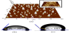
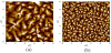
Figure 2 shows the AFM images of the pentacene films grown on the substrates with and without nanostructures on its surface, respectively. It is observed that the pentacene film deposited on the rough surface incorporated with cowl-shaped nanostructures has a different crystallinity with smaller grains than that on the bare cPVP layer. This result indicates that the growth of pentacene molecules is strongly affected by the hydrophobic cowl-shaped nanostructures. The crystallinity of pentacene film was studied by XRD with monochromatic Cu Kα (λ=1.54Å). From the results, we analyzed the thin-film phase ratio of the pentacene films according to the interface conditions as shown in Figure 3, which is defined as [(thin-film phase intensity-bulk phase intensity)/thin-film phase intensity]. For the pentacene film deposited onto the rough surface with nanostructures, the thin-film phase is well maintained without forming bulk phase up to 003 directions. This is of great interest because, in general, the rough surface of gate insulator is expected to deteriorate the ordered growth of pentacene molecules. However, the rough nanostructures in this study facilitated the upright growth of pentacene molecules to the substrate, suggesting that the morphological modification of the gate insulator surface can be a viable method for the ordered growth of organic semiconductors.
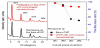
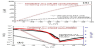
Figure 4a shows the drain current-drain voltage curves (ID - VD) of the fabricated pentacene TFTs according to the interface conditions. The saturation current at a gate voltage (VG) of - 30 V is much higher for the TFT with the nanostructures than for the device without the nanostructures. From the transfer characteristics shown in Figure 4b, the pentacene TFT with the nanostructured cPVP insulator exhibited the on/off current ratio of about 106, increased by about a factor of seven. Most importantly, the field-effect mobility was significantly improved by introducing cowl-shaped nanostructures. In the saturation regime, the calculated field-effect mobility was about 2.94 cm2/Vs for the device with the nanostructured cPVP insulator, cm2/Vs. It is thought that the notable enhancement in the field-effect mobility is mainly attributed to the upright orientation of pentacene molecules because the vertical alignment of pentacene molecules to the gate insulator surface provides a strong Π-Π* overlap [12], increasing the electrical conductivity in the channel direction of TFTs. On the other hand, the threshold voltage (VTH) and sub threshold slope were slightly degraded for the device with the cowl-shaped nanostructures. This is likely to be originated from the interface charges between the pentacene layer and the cowl-shaped nanostructures. Considering that the flat band voltage (VFB) can be approximated to the onset voltage (Vonset) of the device [13], the density of trapped holes can be estimated using Cins (ΔVTH−ΔVFB)/q because VTH above Vonset is an estimate of the trap density in the channel [14], where Cinsis the capacitance of gate insulator; using this approach, the density of trapped holes was found to be about 2.4×1011 cm−2.It is presumed that polyurethane molecules might induce an energetic disorder at the interface. Further investigation is required to elucidate the origin of such interface charges. Accordingly, our results demonstrate that hydrophobic nanostructures on a gate insulator, in spite of deteriorating the surface roughness of an under laid insulator, can open up new strategies for increasing the field-effect mobility in organic TFTs by modifying the growth of organic molecules.
4. Conclusion
In summary, we fabricated the cowl-shaped nanostructures consisting of polyurethane on the cPVP gate insulator and investigated its effects on the pentacene molecular growth and the TFT performance. The pentacene film deposited on the nanostructured cPVP insulator maintained the thin-film phase up to 003 direction without augmenting the bulk phase, indicating that the fabricated nanostructures are conducive to the upright growth of pentacene molecules to the substrate. The pentacene TFTs with the nanostructured cPVP insulator exhibited a notable enhancement in the electrical characteristics. In particular, the enhancement in the field-effect mobility was about a factor of three. Consequently, we suggest that nanostructures formed on the gate insulator can be applied to assist the ordered growth of organic semiconductor molecules, thereby contributing to improving the performance of organic TFTs.
Competing Interests
The authors have declared that no competing interests exist.
Author Contributions
All the authors contributed to the fabrication and characterization of organic devices as well as the interpretation of the results.