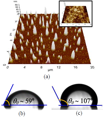
Figure 1:
AFM image of the nanostructured cPVPinsulator(20 μm × 20μm): the inset shows the AFM image of the bare cPVP surface. The side views of sessile drops on (b) the bare cPVP layer and (c) the nanostructuredcPVP layer, respectively.