


1. Introduction
It is ideal for a pipelined processor to run at its full speed when executing an application. However, due to a variety of pipeline hazards, especially the long memory access operations, an instruction thread executed in a pipeline will go through frequent stalls. To lower the long pipeline stall caused by the memory access, we can use cache. Cache reduces the number of memory accesses and effectively shortens the processor stall time. To reduce the impact of execution stall on performance, we can exploit the multithreaded execution. With multiple threads available, the pipeline idle time due to one thread stall can be used by other threads, hence the pipeline throughput is increased.
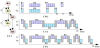
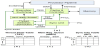
However, when both enhancements (cache and multi-threaded execution) are implemented in the processor system, the synergy may not necessarily exist. Take the problem shown in Figure 1 as an example. Assume two threads (T1 and T2) execute a code segment whose control flow graph is given in Figure 1(a). The code consists of five basic blocks1, B1-B5. Among them, B2 and B4 are loop blocks (the loop counts are shown beside the blocks). Assume that each basic block can be fully cached and the cache is direct-mapped and can hold maximally two blocks. Then, blocks B1, B3 and B5 will compete for one cache location, and blocks B2 and B4 for the other location.
1A basic block contains a sequence of instructions. If the first instruction in the basic block is executed, the rest of the instructions will be sequentially executed.
Assume each basic block takes the same amount of time to execute and the memory access delay (i.e. cache miss penalty) is three times the block execution time. The execution timing of each individual thread is shown in Figure 1(b), where each timing block in the diagram represents the execution time of a basic (instruction) block. For a loop block, the block execution time is multiplied by the number of loop iterations for the overall execution time. The execution trace for thread T1 is B1-B2-B4-B5, and for thread T2 is B1-B2-B3-B5. The two threads have a total execution time of t1+t2. If the two threads are interleaved, without considering any potential cache competition issues between threads, the ideal multi-threaded execution would be like in Figure 1(c). The shaded blocks show the time spent on switching execution to the other thread. The overall execution time is t3 and (t1+t2)≥t3 >max{t1, t2}. However, since the two threads compete for locations in the cache, one thread may evict the instructions cached by another, and the real threaded execution turns out to be the one that is shown in Figure 1(d). As can be seen, the number of cache misses, hence the thread switching frequency, is actually increased, so is the execution time (t4 > t3). Cache misses lead to accesses to memory. Since memory access is power consuming, significant power will be consumed. In addition, the thread switching incurs overhead, which further adds woes to the design.
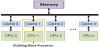
In this paper, we investigate the micro-architectural level solutions to make the cache behave in harmony with the threaded execution in the pipeline. Since instruction cache misses account for a considerably higher performance impact than data cache misses [1] due to frequent instruction fetches, we focus this study on the instruction cache. We target applications that offer embarrassing parallelism where the same code can be executed by a number of independent threads on different data sets. Such applications can be found in real-world computing problems such as encryption [2], scientific calculation [3], multimedia processing [4] and image processing [5]. Those large computing problems demand designs of multiprocessor systems that can be built on the small building-block processors like the one we discuss in this paper, as is illustrated in Figure 2. Such embedded processors are usually constrained with resources to reduce energy and area costs. We focus on the multi threaded processor with a single pipeline and a small cache that processes light weight applications and we present a thread synchronization approach that synchronizes thread execution on frequent loops to enhance loop instructions reuse. We introduce a novel cache design with a cache locking scheme that provides a near 100% cache hit for synchronized thread executions and we apply the thread switching design introduced in [6] that parallelizes tasks in the thread scheduling and tucks-in execution switching into the processor pipeline to eliminate the thread switching performance overhead. Overall, our design is small, low cost, yet of high performance and energy efficiency.
2. Related Work
Thread synchronization and cache locking have been studied in several areas. Works on thread synchronization can be commonly found at the system level implementations, where operating system or special firmware coordinates and synchronizes threads execution to ensure the overall applications’ functionality and performance [7-9].
Synchronizing threads to increase instruction reuse (hence reducing cache misses), has also been investigated recently in some application areas, such as database processing, cryptography, image processing and multimedia processing. This section is aimed at discussing some of these studies that are relevant to our work.
Atta et al. in [10] investigated online transaction processing (OLTP), where each transaction can be regarded as an independent execution thread. Some transactions execute similar functional code. They proposed to synchronize those similar transactions to optimize instruction cache reuse for better performance. They presented a hardware level synchronization scheme, STREX, that is fully transparent to the program-mer. This scheme exploits similar behavioural patterns within transactions to attain an optimal instruction reuse level in a single core. The points at which the transaction executions are switched, are dynamically detected. STREX groups transactions of the same type into teams and places them in a queue for a CPU. The first transaction of the queue is flagged as the lead and a counter named phase ID is used to indicate the code section that is synchronized. The lead transaction executes first and fetches all instructions of a synchronization section into the cache. The cached instruction section can then be used by the following transactions, avoiding repeated memory accesses. Transactions are executed in a round robin manner. When the current synchronization section is finished, the lead transaction increments the phase ID and moves execution to the next section. Once all transactions of a team finish execution, the processor starts executing the transactions of another team.
A similar hardware level thread synchronization mechanism was also proposed by Nickolls, et al. [11]. In their work, application threads that execute the same pool of instructions on different data sets are grouped together into an array called Cooperative Thread Array (CTA). A sequence of synchronization points called barrier instructions are predetermined for each thread group. Barrier instructions are detected by hardware and used to suspend execution of threads until a specified number of threads reach that barrier point. This approach is designed for large, high power consuming graphic processing subsystems where very high thread level parallelism is available. Utilization of synchronization points (SP) has also been explored in the recent work of Foo [12]. In this work, synchronization is used to manage access to shared resources by simultaneous threads. Every thread in the system pauses at the SP and once all the threads are arrived at that SP they start executing simultaneously. However, due to varying execution flows controlled by branch instructions, some threads may miss a specified SP. When this happens the threads that miss the SP are flagged. Threads that are paused at the SP will wait only for the non-flagged threads. In order to synchronize flagged threads, an extra SP is set at the return address of the branch. Apart from the above mentioned work, hardware approaches to provide synchronized access to data cache are also studied in some recent research work. Zhang, et al. [13] examined data reuse through thread scheduling for data centres that concurrently execute multiple dataintensive threads. They use a technique, called Cache Matching, to capture data locality within and across threads. With their method, parts of in-coming cache request sequences are stored in a small buffer and interleaved such that a high cache hit rate is attained. Huang, et al. [14] devised a dynamic thread scheduler to co-optimize data cache locality and load balance in general purpose graphic processing units (GPGPU) that implement an on-chip shared cache structure. Rogers, et al. [15,16] also proposed a hardware mechanism called cache-conscious wave front scheduling (CCWS) to synchronize accesses to the first level data cache to avoid potential cache thrashing. It helps to reduce power consumption and is especially effective for massively multi threaded processor architectures such as GPUs. All of the above designs use hardware to control thread synchronization at the task level for cache locality. In this paper, we consider thread synchronization at the loop execution level and the hardware control of thread synchronization can closely work with cache to achieve high reuse of cached code. Instruction cache locking is a technique employed in our work to prevent loop instructions from getting evicted during loop execution. This technique has been discussed in several studies, where cache locking is mainly used in reducing the timing unpredictability in hard real-time program execution. By locking certain data in cache, the fluctuation of the related cache misses and memory access time can be controlled. Liang and Mitra [17] proposed a static instruction cache locking algorithm that uses the cache temporal re-use profile of a program to determine the most beneficial instruction cache blocks to be locked. In a similar work Liu et al. [18] presented a compiler level instruction cache locking mechanism where instructions to be locked in the cache are determined by the program’s statistical execution information and the locking is statically implemented. With this approach, cache contents to be locked are fetched into the cache before the program execution and remain in the cache until the execution finishes. In [19] Qui, et al. proposed a dynamic instruction locking mechanism that operates in two phases; offline and online. In the offline phase, candidate locking regions are selected based on the weighted control flow graph of the program and the locking profit of each cache block. Candidate regions include loop and non- loop instruction blocks. In the online stage, a branch predictor fetches the cache locking routine instructions of the regions that are predicted to execute in the near future into a buffer. This removes the need to place the cache locking instructions inside the program. Another recent work in line with instruction cache locking is by Anand and Barua [20]. Their mechanism identifies points in the program where a significant shift in the instruction locality occurs and computes the cache lines required to be locked at each point. However, this approach requires special locking instructions inserted into the respective program points. In order to prevent this from altering the original program layout which eventually invalidates the program point calculations, the authors have employed the trampolines approach proposed by Buck and Hollingsworth [21].
All of the above instruction cache locking mechanisms are either software level approaches that require customized instructions to be added into the application thread and/or involve complex computations to be performed before the execution of a program.
In our work, we incorporate thread synchronization and instruction cache locking into the multi threaded execution in a single pipeline for high instruction cache locality. Our approach is hardware based and has a configurable synchronization control. It is purely transparent to software, yet still provides some customization flexibility for a given application. With our approach, high instruction cache locality can be achieved even with a small size of cache.
3. Design of Thread Synchronization for High Instruction Cache Locality
Usually loops account for a significant part of the overall execution time. To improve the instruction cache locality, we aim at the loops with a high execution frequency. We want thread executions synchronized at such a loop so that once the loop is cached by one thread, it is available in the cache for other threads, avoiding repeated memory accesses.
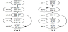
An application can normally be represented by a control flow graph (CFG) as illustrated in Figure 3(a). In CFG, a node represents a basic block that contains a sequence of instructions. If an instruction in the block is executed, all instructions of the block will be executed. The CFG of an application shows how execution flows from one basic block to another. We name such a block an instruction block, or IB. Every instruction resides in a corresponding block in the memory. An IB may occupy a number of memory blocks (MB). For example in Figure 3(a), the instruction block B1 that contains three instructions with addresses 0000 to 0010 given inside the block, will occupy two memory blocks if each memory block holds two instructions. When the IB is executed, the related MBs will be accessed.
To effectively capture the correlation of the thread execution and memory access pattern, we use a memory trace graph (MTG), where each node represents the set of MBs accessed for an IB. The MTG diagram specifies how the execution walks over the memory space from one MB to another. As an example, Figure 3(b) shows the corresponding MTG of the CFG given in Figure 3(a). In this MTG, each value in the node is the address of an MB, and each block holds two instructions. As can be seen, two IBs can overlap on an MB in MTG.
An early thread that comes to a loop for synchronization should wait until other threads have arrived. When the loop is cached, it will be locked until the loop is completed by other threads. We call such a loop the sync loop, the thread that has arrived for the sync loop execution the sync thread, and the point at which a sync thread is waiting for other threads for next action a sync point. For thread synchronization, multiple sync points may be needed. A proper design of cache, cache locking and sync points are critical for the sync loop execution, which is discussed below.
The effectiveness of cache locality is dependent on whether the cache can hold the whole sync loop. For a given application, assume the largest sync loop occupies M MBs in the memory, in order to have a sync loop fully cached, the minimal cache size is,
where
There are many sync loops in an application and some sync loop sizes may be smaller or much smaller than the largest sync loop. To allow for maximal cache availability to other non-sync threads, during a sync loop execution, we only partially lock the cache for the sync loop.
Cache locking can be performed on a block basis or on a segment basis (a segment covers blocks that are required for the sync loop). In the block-based locking, each block is individually locked. An extra
bit for locking state is required for each block in the cache. During a sync loop execution, when a block is cached, its locking bit is set. After the sync loop execution is completed, the cache controller will reset all the locking bits to free the cache blocks for different memory data. This design is not scalable as the extra locking bit requirement may incur considerable amount of resource overhead for a complicated application with a large cache.
For the segment based design, the whole section of blocks that hold the loop are locked at the same time. After the segment is locked in the cache, each time a memory access brings a block to cache, the block location is checked against the lock section range. If it is within the range, the write of the memory block to the cache is disallowed. This design can be implemented with a fixed logic (two registers for the start and end points of the cache segment plus a comparator), hence scalable. We therefore use segment locking method in our design.
The cache segment is expected to be locked by the thread that first executes the loop so that the loop instructions cached can be reused by other sync threads. However, for a sync loop that contains conditional execution paths, some instructions may not be executed by the first thread, hence not be cached. This complicates the cache locking control.
To ensure all instructions in a sync loop are cached, we employ prefetching and a prefetch buffer in the cache design. We set threads to be assembled at the first block of the loop and we call the address of the first block the assembly point, AP. Once the first sync thread arrives at AP, prefetching is activated and starts to fetch the loop instructions into the buffer. The buffer serves as a temporal repository so that the prefetched instructions will not be evicted from the cache by other non-sync threads before the loop starts. The buffer can be small but should be big enough to ensure the whole loop is cached during the first sync loop execution. After all threads arrive at the AP, the buffered instructions are transferred to the cache and the freed buffer entries are refilled with new instructions by prefetching; Both the instruction transfer and buffer refill can be performed in parallel and this parallel processing also helps to reduce the buffer size2. When the loop is fully cached, the cache segment related to the loop is locked. We call this cache locking approach prefetching-then-cache-locking, PTCL.
2In our designs for a given set of applications, the buffer size is 32 bytes.
We use the address of the last memory block in the loop as the locking point, LP. Once the prefetching passes the point, the loop is immediately locked in the cache.
Upon completion of a segment locking, the cache locations of the corresponding assembly point (AP) and locking point (LP) are written to a register pair as the start and end point of the cache segment. In case a new memory block is fetched, the cache controller checks its mapped cache location. If it falls in the locked range, the new memory block will not be cached.
For a sync loop on the conditional path, such as loop block B4 in Figure 3(a), some threads may skip the loop and take different execution paths. Those threads should be dynamically detected and excluded from the loop synchronization. We set the first instruction on the path that is parallel to the conditional sync loop as a bypassing point, BP. If a thread passes this point, it is removed from the sync loop execution. There may be multiple parallel paths, hence multiple passing points, for a sync loop.
During the sync loop execution, when a thread finishes the loop, the execution will switch to another thread. We use the address of the last instruction of the loop as the control point for thread switching. We call this control point the switching point, SP.
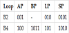
As an example, Table 1 lists the four sync point values for the two loops B2 and B4 in Figure 3(a). Both AP and LP are block addresses, and BP and LP are instruction addresses. Since B2 does not sit on a conditional path, BP is not applicable to B2.
We apply the above synchronization design into the multi-threaded processor design, which is detailed in the next section.
4. Multi-Threaded Processor With Sync Loop Execution
Our design is based on the multithreaded processor that takes zero clock cycle for thread switching, proposed in [6]. The basic idea of this design is to perform thread switching in parallel to thread scheduling and keep the scheduling logic out of the critical path.
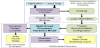
We extend the baseline design by adding the sync control unit and modifications to the thread switching control and cache design, as shown in Figure 4(a). The thread switching control now takes the loop synchronization into account and the cache controller includes the logic for prefetching and cache segment locking.
To dynamically control the sync loop execution, we use a table to record the state of each thread as shown in Figure 4(b). Each thread has a ready bit, sync bit, and a bypass bit for conditional loop execution. We call this table the thread state table, TST.
The ready bit of a thread indicates whether the thread is ready to execute. This bit is set under one of the three cases: 1) when the memory request from the thread has been completed (i.e. the missed block is now available in the cache), 2) when a sync loop is set to start, or 3) when a sync loop is completed by all threads.
The ready bit is unset also in three cases: 1) when the thread encounters a cache miss, 2) when the thread is stopped at a sync point (AP/SP), or 3) The thread finishes its execution.
The sync bit of a thread is set when the thread execution has reached the assembly point and it is unset when the thread finishes with the sync loop. We use the sync bit to control the sync loop execution, while the ready bit is used by the thread scheduler for the next thread switching.
The bypass bit is used to identify whether the thread has taken an alternative path bypassing a conditional sync loop. If so, the bit is set and the thread does not participate in the sync loop execution. It is unset when the sync loop is finished. Initially, the bypass bit is set to zero. If loop bypassing happens by an instruction in the AP block, the related thread will first stop at AP and later be detected when it passes BP. When it passes BP, the bypass bit is set. The size of TST is decided by the number of existing threads.
Since each thread can cause a cache miss, at a given moment there may be multiple requests for memory access. These requests are recorded in a memory request queue (MRQ), as shown in Figure 4(c). For each request, the thread that incurs the memory request and the address for the memory access are specified. An entry is reset if the related memory data is fetched from the memory.
For a given application, there may be many sync loops. We use a sync information table, SIT to store the sync points for such loops, as shown in Figure 4(d). For each loop, AP, LP, SP and BP (for conditional execution) are provided. A pointer is used to point to the next sync loop. The SIT table can be reconfigured, which offers the design flexibility for different applications.
The thread state table is updated by the sync unit, cache controller, and the scheduler as elaborated below.
The sync unit takes as input the processor PC value and the sync point values of a loop from the sync information table, and generates the three control signals for the following purposes:
- to update the thread sync state,
- to start sync loop, and
- to enable prefetching-then-cache-locking (PTCL).
The sync unit consists of three components: logic for checking threads bypassing the conditional loop, logic for assembling threads, and logic for starting the loop execution. The operations of each of these components are specified in Algorithms 1, 2 and 3 respectively. The comment lines in the algorithms explain the related operational steps. For readability and conciseness, functions are used to hide some calculation details and their implementation should be straightforward. For example, Function getSyncThreadsNum() can be implemented by counting the number of threads that have the ready bit equal to 1. Variables bypass(j), sync(j) and, ready(j) are bit values given by the thread state table (TST).
In the three algorithms, PC stands for the current instruction address from the processor. Since thread assembly uses a block address as the assembly point (AP), the block address of the PC value, denoted as PCBLK , is used in Algorithm 2.
As it is elaborated in Algorithm 2, when the first thread arrives at AP, prefetching of the loop blocks starts. When all threads are assembled, the sync loop execution is enabled (i.e. the control signal loop-en is set). The control of the sync loop execution and prefetching are detailed in Algorithms 3 and 4. Algorithm 3 describes how a sync thread is executed. Function getFinishedThreadsNum() gets the total number sync threads that have finished the loop. If there are unfinished threads, the execution will switch to another unfinished thread once the current thread completes. Function get Finished Threads Num() is simply a counter that increments when a thread reaches the SP and resets when the sync loop execution starts..
Algorithm 1: Check Bypassing Threads
/* bypassChecking(i,j): Check if thread j bypasses the conditional loop i */
if BP(i) =6 0 then
/* For each new PC, check if the current thread j bypasses the
loop i */
if PC = BP(i) then
/* Set thread j as a bypassing thread and exclude it from loop
execution*/
bypass(j)=1;
sync(j)=0;
end if
end if
Algorithm 2: Assemble Threads
/* threadAssembly(i): Assemble threads for sync loop i. */
/* The total number of threads is m.*/
/* For instruction address PC, PCBLK is the block address.*/
for each new PC do
if PCBLK = AP(i) then
/* Set current thread j as a sync thread */
sync(j)=1;
/* Get the number of sync threads, S */
S = getSyncThreadsNum();
/* Get the number of bypassing threads, P */
P = getBypassingThreadsNum();
/* If first thread to arrive at AP, initiate prefetching */
if S = 1 then
prefetch(AP(i), LP(i));
end if
/* If all threads not synced, stall the current thread */
if S < m−P then
ready(j)=0;
else
/* If all threads synced, enable loop execution */
for every thread, k do
if sync(k)=1 then
ready(k)=1;
end if
end for
loop-en=1;
end if
end if
end for
Algorithm 3: Sync Loop Execution
/* Execution of sync loop i.*/
while loop-en=1 do
for each new PC do
/* If the current thread completes the loop, reset the thread
sync bit. */
if PC=SP(i) then
/* Reset the thread sync bit */
sync(j)=0;
/* Get the number of completed threads, F */
F = getFinishedThreadsNum();
/* When all threads complete the loop, exit from the sync
loop execution*/
/* Else stop the thread and switch to the next sync thread */
if F = S then
loop-en=0;
lock-en=0;
/* Set all sync threads ready */
for every thread, k do
if sync(k)=1 then
ready(k)=1;
end if
end for
else
ready(j)=0;
end if
end if
end for
end while
Algorithm 4: Prefetching Control
/* Prefetch from block a to b for sync loop execution */
A=a;
/* On each clock cycle, */
while A <= b do
/* If prefetch buffer is not full and no memory read is currently
happening, send a memory access request for block A */
if (buffer not full) and (no mem read) then
memRequest(A);
A = A+1;
end if
end while
/* if all the memory requests are complete, lock the cache */
if A = b+1 then
lock-en=1;
end if
Algorithm 5: Cache Controller
/* When block A misses in the cache, send the request to memory
request queue (MRQ). IF A already exists in MRQ, only add the
thread ID to the existing entry. Else, add the whole entry.*/
if miss(A) then
MRQ(A)
end if
/* Dispatch requests to memory on each memory access cycle */
/* If the memory request queue (MRQ) is not empty*/
if MRQ is not empty then
for every block address in MRQ, B do
/* if the request is not restricted by cache locking, send the
request on to the memory bus */
if (lock-en =0) or (lock-en=1 and (B< SP or B> LP)) then
accessMem(B);
end if
end for
end if
/* On reading block from memory address C */
/* Reset the mem-request-field and the related threads ready */
mem-hit(C)=1;
for every entry i in MRQ do
if MRQ(i,address)=C then
ready(MRQ(i,thread))=1;
MRQ(i)=0;
end if
end for
Algorithm 4 describes the prefetching control. There are two registers associated with the prefetching unit. The prefetch buffer sends its state (full/not full) to the prefetch unit. It also receives the current memory read state mem read/no mem read from the cache controller.
When prefetching is enabled, the prefetching unit sends the memory requests every time the buffer state is not full and the current memory read state is no mem read. The unit then monitors the completion of each request. When the last block is cached, the unit enables cache locking (lock-en=1). In the algorithm, a, b and A represent memory block addresses.
Algorithm 5 shows the operation of the instruction cache controller to manage access to the instruction memory. The memory request queue (MRQ) resides in the cache controller. As shown in Figure 4(c), it consists of a list of memory block addresses waiting to be fetched into the cache and IDs of threads that issued each of these requests. In Algorithm 5, MRQ(i,address) represents the block address at the ith entry of the MRQ whereas MRQ(i,thread) represents the thread IDs at the ith entry of the MRQ. A, B and C represent memory block addresses. The algorithm consists of three parts: 1) adding a request to the MRQ upon a cache miss, 2) dispatching requests from MRQ to the memory, and 3) reading a block into the cache.
5. Experiments and Results
To evaluate our design, we set up a simulation platform, as shown in Figure 5. Our baseline design utilizes a five-stage single pipeline that implements the PISA [22] instruction set architecture. The multithreaded processor can handle a maximum of four independent threads. It consists of a one-level instruction cache.
For a given application, its loop information can be extracted from profiling, and this information is used to configure thread synchronization control. Program and data binaries obtained by compiling the application are placed in instruction and data memories of the multi-threaded processor hardware model. For profiling and compilation purposes Simplescalar [22] tool set is used as it can natively emulate the PISA instruction set.
The area, power and delay of hardware components are estimated by Synopsys Design Compiler [23] with the TSMC Standard 65 nm Cell Library [24]. The same 65 nm technology is also adopted for our memory model. The critical path delay (2.2 ns obtained from synthesis) is used to determine the clock cycle time. The time and energy consumption per memory access is obtained by CACTI [25] for different memory sizes. Multi-threaded executions are simulated with the Modelsim simulator [26], from which CPI, cache misses and thread switchings are obtained.
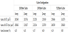
Table 2 shows the kernel benchmarks used in our experiment. Those kernel benchmarks can be found in many applications in the areas of graphic processing, signal processing and cryptography. The first column of the table lists the benchmark names. Their abbreviations and code sizes in kilobytes are given respectively in the second and third columns. The last column shows the cache size selected for each of the benchmarks. The choice of the cache size is dependent on the size of the available frequent loops and we select the minimal cache size required to fully hold the sync loops. For the given set of benchmarks, the sizes of the small caches used are 128-bytes, 256-bytes and 512-bytes.
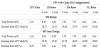
The latency and dynamic energy consumption per memory access estimated by CACTI are shown in Table III. For the access latency (in nanoseconds, ns), the equivalent number of CPU clock cycles (cc) is also given in Column 3 of the table.
We incorporate the memory access delay cycles into the processor hardware model simulation in ModelSim. For each benchmark, we simulate the application execution using three execution methods:
- Single threaded execution (ST),
- Baseline multi-threaded execution (MT), and
- Multi-threaded execution with sync loop (MT-Sync).
In the ST execution, the threads execute in the pipeline sequentially (ie. thread n starts to execute only after thread n-1 finishes its execution). Since there is no interleaving of threads, every time a cache miss occurs the pipeline will go idle until the memory access finishes. MT is implemented on a baseline multi-threaded processor with the round-robin thread selection policy and MT-Sync is implemented on the same multi-threaded processor with hardware extensions for synchronized thread execution on frequent loops. For a given application, the working set of all three execution methods is the same.
Two typical cache configurations: direct mapped (1-way) and 2-way set associative cache are implemented in each of the three designs. Since the cache size is small, higher associative caches may give diminishing returns on energy savings. Therefore they are not considered here.
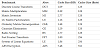
Memory cache significantly impacts the power consumption of the processor. Increase in power consumption depends on the configuration of the cache as well as the multi-threaded processor design. Table 4 shows the total power (in milliwatts, mW) of MT and MT-Sync processor designs with and without a cache and percentage increase in power consumption caused by the addition of caches. Here we consider six cache configurations used by the benchmarks of this experiment. The total power is the aggregate of total dynamic power and cell leakage power.
As can be seen in the table, for all cache configurations, the increase in power consumption caused by the addition of the cache is significant ranging from 18.77% to 25.87% for the 128-byte caches, 34.45% to 48.18% for the 256-byte caches and 65.54% to a whopping 83.82% for the 512-byte caches. This shows the rapidly increasing impact of cache size on the power consumption of the system. This motivates the need for the use of small caches for low power processors.
Similarly, implementation of the MT-Sync design introduces extra costs to the system in terms of power consumption and area. The last row of Table 4 shows the percentage increase in total power of MT-Sync implementation compared to that of MT. These additional power consumption costs lie in the range of 4.41% to 10.47% for the considered cache configurations. However, the savings due to the cache miss reduction from MT-Sync design outweigh these overheads, leading to an overall improvement on design energy efficiency.
Table 5 shows the on-chip area of MT and MT-Sync processor implementations. The last row of the table shows percentage increase in area caused by the synchronization hardware. It can be observed that percentage area increase ranges from 3.85% to 4.25% depending on the cache con-figuration.
As can be seen from Table 3, the memory access latency and energy consumption per access (hence the performance and the energy consumption of the overall system) vary with the memory size. In the next two subsections we analyse the effectiveness of MT-Sync execution in terms of performance and energy consumption under two instruction memory size settings; fixed memory size and varied memory size.
5.1 Experiments on designs with fixed memory size
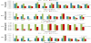
We first test the designs with a fixed off-chip instruction memory size. For this experiment we select a moderate memory size of 300MB from the list given in Table 3. For this size, each memory access takes 10 clock cycles. The CPI, cache misses, thread switchings, and energy consumption data obtained from simulations with a direct mapped cache for each benchmark under three different designs, ST, MT, and MT-Sync, are shown in Figures 6(a), 6(b), 6(c), and 6(d), respectively. The average values of each of the measures over all benchmarks are also presented in the last bar group (labelled as AVG) in each figure. For a neat presentation, in Figure 6, cache miss, thread switching, and energy consumption are normalized to the ST design, but the actual data (namely, the number of cache misses, the number of thread switchings, and the energy consumption in μJ) for average values are also given inside the brackets in the figure.
The energy consumption is the sum of energy consumed by the processor and the memory, as given in the formula below.
where E stands for the energy consumption; P is the total power consumed by all components, except the memory, in the processor system (Figures 4), T is the application execution time; e is the energy consumption per memory access, and m the cache misses. For every application, ST, MT and MT-Sync executions process the same data set. Based on the same data set, we are able to compare the three designs in terms of CPI, cache misses, switching counts, and energy consumptions, as given in Figure 6.
From Figure 6(a), we can see that the MT design under-performs, with an average CPI of 2.26, higher than the values of 2.09 and 1.41 from the ST and MT-Sync designs. This is due to the extra cache misses incurred by the thread execution, which is verified by the data shown Figure 6(b). In most cases, MT has a higher cache misses than other two designs and on average it is 35% higher than the ST execution. On the contrary, the MT-Sync design reduces the cache misses by 27% as compared to the ST design. It can also be observed from Figure 6(c), the MT-Sync design incurs less thread switchings than the MT design where about 46% average saving can be achieved.
The improved performance and reduced cache misses help reducing the energy consumption. As can be seen from Fig-ure 6(d), the MTSync design consumes less energy than MT and ST designs; for MT, in most cases extra energy consumption has been incurred. The average energy consumption of MT-Sync is 32 μJ, considerably lower than those from ST (54 54 μJ) and MT (80 μJ) However, with application FFT, although there is a 13% improvement in performance, the high number of cache misses lead to more energy consumed. The increased number of cache misses is caused by the existence of pingpong effect due to ineffective thread interleaving at a number of points outside of the frequent loop execution. this issue is mitigated by using 2-way set associative cache as manifested by the results shown in Figure 7 for the designs when 2-way associative cache is used.
Compared to the 1-way cache, the 2-way cache improves the performance (CPI, caches misses, thread switchings) of both MT and MT-Sync designs except in the case of AES. On average, MT-Sync offers the highest overall performance and lowest energy consumption among the three designs.
5.2 Experiments on designs with varied memory size
The size of the off-chip instruction memory can have a significant effect on performance and energy efficiency. As the memory access penalty varies with the memory size, the thread interleaving patterns, hence the execution time and number of misses vary. Moreover, large memories consume more power pushing up the energy consumption. The size of the off-chip memory depends on the applications run on the system and the overall system architecture. In these experiments we focus on single building block embedded processors that go in large multiprocessor systems. At this point, our mechanism is oblivious to the architecture of this multiprocessor system; hence it is infeasible to specify an exact memory size. Therefore, for fairness, we investigate the effectiveness of our synchronization design for a range of possible memory sizes.
In order to do this, we repeat the same set of experiments for designs under ten different memory sizes, ranging from 50MB to 500MB as shown in Table 3. In these experiments, a large set of data for CPIs, cache misses, and thread switchings are collected.
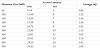
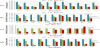
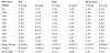
To introduce the metrics used to analyse the variations in performance and energy consumption, we use one benchmark as an example. Table 6 lists the CPI readings for the bench-mark, LE. For ease of observation, the data in the table are also presented in Figure 8. As can be seen in the figure, generally, the CPI shows an increasing pattern with the memory size (due to increased memory access time) for all designs. Occasional CPI drops can be attributed to the drops in cache misses due to the changes in the thread interleave execution pattern. To save the space and facilitate the design comparison, we apply the linear regression on the experiment data for each benchmark on a given design. For example, the dashed line in Figure 8 is the regressed CPI linear line (linear trend line) of the MT-1way design for LE . We use the slope of the linear line to evaluate the effectiveness of a design to mitigate the impact of long memory access penalty on the overall performance, and we use the average value to consolidate the collected data from the experiment. We also calculate the regression error of the actual CPIs from the linear trend line. The lower the regression error, the more linear the actual CPI increase, hence more predictable.
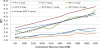
These three values: regression error (Reg. Error), linear slope, and the average, for LE application are shown in the last three rows of Table 6.
By analysing the results shown in Table 6 and Figure 8, following conclusions can be made:
- Average CPI values show that the MT-Sync execution produces higher performance than both ST and MT executions.
- The slopes of the linear trend lines show that for every cache configuration, when memory size increased, the increase of the CPI from the MT-Sync execution is slower than those from ST and MT.
- The error of linear regression of the MT-Sync execution is less than that of MT execution for both cache config-urations which goes on to suggest that performance of MT-Sync is more predictable than that of MT.
Similarly, we calculate regression error, linear slope, and the average values for all benchmarks under ST, MT and MT-Sync designs implemented with direct mapped (1-way) and 2-way set associative caches. Table 7 shows the complete set of the calculated values. In this table, Cache Assoc. is the number of ways in a set, App. stands for the application name, Avg. the average CPI, and Reg. Error the linear regression error.
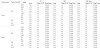
The results of the designs with 1-way cache are given in the top half of the table and the results of the designs with 2-way cache are given in the bottom half of the table. The average values over all benchmarks are given in the last row (as highlighted) in each half. As can be seen from this table, with the 1-way design, MT-Sync offers higher performance than other two designs over the varied memory sizes, with an average CPI of 1.39, lower than those from ST (2.09) and MT (2.31) When the cache associativity is increased to 2-way, the CPI of ST is increased; this is due to increased cache misses and for each miss, the related pipeline stall time cannot be utilized in the single thread execution. But since the stall time can be exploited in the multi-threaded execution, the CPIs of MT and MT-Sync are reduced. Moreover, based on the regressed CPI linear line, MT-Sync has the smallest slop, which means it can effectively mitigate the long memory access penalty for large memories, and this trend is also more predictable than that of the MT execution because of the smaller regression error.
Table 8 shows average (over 50MB-500MB different memory sizes) cache misses, energy consumption (in micro-joule), and the switching count for the multi-threaded execu-tion. As can be seen from the table, MT sometimes incurs extra cache misses as compared to the single threaded execution, but with thread synchronization (MT-Sync), the cache misses are reduced. Overall, MT-Sync consumes less energy (an average of 29.41μJ) than the ST (60.07μJ) and MT (69.28μJ) designs. It can be also observed that both MT and MT-Sync benefit from the 2-way cache, with the reduced cache misses, thread switching count, and energy consumption.

6. Conclusion
Cache and multi-threading are two typical design techniques for performance improvement. But when they are implemented in a processor, they can adversely interfere with each other, leading to reduced performance and increased cache misses and power consumption.
In this work we investigated multi threaded processors with an instruction cache for applications that have embarrassing parallelism (the same code can be executed by a number of in-dependent threads on different data sets). Such multi-threaded processors can be used as building blocks in constructing a large multiprocessor system.
We targeted the frequent instruction loops (sync loop) for high temporal locality. Threads are synchronized on the sync loop. During the sync loop execution, the sync threads can be interleaved with nonsync threads, and the cache locking is used to prevent the non-sync threads from evicting the cached sync loop instructions.
We presented a micro-architectural level thread synchronization design to synchronize threads and interact with cache locking for sync loop execution. The thread synchronization design uses a prefetch based cache locking mechanism (PTCL) so that high cache locality can be achieved even with small caches. To reduce the thread switching overhead, we applied a parallel and tuck-in (PTL) approach for thread switching control with which zero-switching delay can be achieved with the explored processor.
To verify the effectiveness of our design, we run experiments on a set of kernel applications. The experiment results on a set of benchmarks show that the thread synchronization indeed helps reducing cache misses, avoiding unnecessary thread switchings and improving overall performance and energy efficiency. For the designs with 1-way cache and 300MB memory, an average of 26% baseline energy can be saved as compared to the 37% energy overhead caused by the baseline MT design, and the energy savings become more significant when the memory size is increased.
It is also demonstrated that the synchronization helps to mitigate the impact of long memory access delay on the overall performance, making the MT-Sync design more scalable than the traditional multithreaded design.
Competing Interests
The authors declare that they have no competing interests.