


1. Introduction
Thermoelectric (TE) materials are among the important potential
candidates for alternative and complementary sources for energy,
wherein heat can be directly converted into electrical energy and vice
versa [1]. Efficient TE materials should exhibit a high thermoelectric
figure of merit defined as ZT=S2T/(ρκ), where T, S, ρ, and κ are
the absolute temperature, Seebeck coefficient, electrical resistivity
and thermal conductivity, respectively [2]. Among the traditional
thermoelectric materials, Bi2Te3-based materials, including p-type
(BixSb1-x)2Te3 and n-type Bi2Te3-ySey, are well known as the most
efficient TE materials that operate near room temperatures [3,4].
Bi2Te3 has a rhombohedra structure with the space group
Several methods have been used to obtain isotropic Bi2Te3-based bulk materials. For example, by sintering nano-sized spherically shaped powder synthesized via chemical reaction method, Kim et al. [6] obtained isotropic p-type Bi0.5Sb1.5Te3 bulk sample that had no directional difference in TE properties, and the ZT value of 1.1 in both parallel and normal to the consolidated direction was obtained. Through ball milling and hot pressing of Bi2Te3-based n-type single crystals, isotropic ZT had been achieved for Bi2Te2.7Se0.3 bulk sample with the peak ZT of 0.85 in both directions parallel and normal to the pressing direction [8]. Unfortunately, although there have been a few reports related to the preparation of isotropic Bi2Te3-based alloys, the obtained ZT values for the isotropic materials are not high to meet the requirements of large scale applications. As a matter of fact, to achieve isotropic superior thermoelectric performance for Bi2Te3-based alloys with good mechanical properties, one needs not only to reduce (or eliminate) the anisotropy in their microstructures, but also to enhance (or maintain) both power factor (PF) and phonon blocking in Bi2Te3- based alloys. In this aspect, nano-inclusions have been shown to be efficient. They are found to be able to simultaneously scatter the phonons and filter the lower-energy carriers so that both the power factor and thermal conductivity contributions could be synergistically improved [10,11]. To our knowledge; however, the attempt to achieve superior thermoelectric performance for Bi2Te3-based alloys in different measured direction is not successful until today [6].
In the present work, isotropic microstructure and high ZT are obtained for (BixSb1-x)2Te3 with x=0.16, 0.18 and 0.20 in the both measured directions. The largest ZT=1.37 (at 416K) are achieved for (Bi0.16Sb0.84)2Te3, which is attributed to both the lowering of k from enhanced phonon scattering due to Sb2O3 nano-inclusions and the elevated S via intensified energy filtering effect from interphase potentials. In addition, the compression strength for (Bi0.16Sb0.84)2Te3 in this work is 60MPa and 65MPa in the two measured direction, which is six folds and 1.60 times as larger as that of commercial ingot parallel and normal to the directional solidification direction, respectively.
2. Experimental Section
2.1 Sample preparation
Elemental Bi (99.99%, Alfa Aesar), Sb (99.5%, Sigma Aldrich) and Te (99.999%, Alfa Aesar) powders are weighted according to the formula of (BixSb1-x)2Te3(x=0.16-0.24) doped with 3 wt% Te. The powder mixture is loaded into quartz ampoule sealed under vacuum at 10-2 Pa, and then heated at 800°C for 10 h. Then the ingots are ground into powder by using a mortar for one hour.
The powders about 28g are compacted by spark plasma sintering (SPS)at a pressure of 50 MPa in a diameter of 20 mm graphite mould in vacuum for 5 min. The sintering temperature, heating rate and cooling rate are 673 K, 373 K/min and 373K/min, respectively. After SPS, bulk samples with dimensions of cylinder 20 mm od × 12 mm length are obtained.
2.2 Microstructure characterization
The sample is characterized by X-ray diffraction (XRD) using Philips X’Pert PRO X-ray diffractometer equipped with graphite monochromatic Cu Kα radiation (λ= 1.54056 Å). The operation voltage and current are kept at 40 kV and 400 mA, respectively. TEM (transmission electron microscope) observations were performed on a JEOL-F2010 instrument with an acceleration voltage of 200 kV. The morphology is characterized by field emission scanning electron microscopy (FESEM; SU8020).
2.3 Measurements of thermoelectric properties and mechanical properties
A commercial four-probe apparatus (ULVAC-RIKO ZEM-3) is applied to measure the electrical resistivity and Seebeck coefficient of the bar samples. The thermal diffusivity D is obtained by a laser flash method (Netzsch LFA-457) performed on rectangle samples. The specific heat, Cp, is determined from the DSC measurement (Pyris Diamond DSC, Perkin-Elmer). The thermal conductivity is calculated from κ =DCpd, where d is the density of the sample determined by Archimedes’ method. The hole concentration at 300K is measured using a physical properties measurement system (Quantum Design). The measurements of room-temperature compression strengths of the samples are carried out on Instron 3369.
3. Results and Discussion
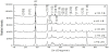
Figure 1 shows the X-ray diffraction (XRD) patterns of bulk
samples sliced normal (
The low-magnification FESEM image for (Bi0.16Sb84)2Te3 fractured normal to the pressing direction (Figure 2a) reveals that a large number of small particlesare randomly embedded among the particles with micron dimension. A high-magnification FESEM image (Figure 2b) demonstrates that thesmall particles are around the size of 30-80 nm. The low-magnification FESEM image for (Bi0.16Sb84)2Te3 fractured parallel to the pressing direction (Figure 2c) reveals many small dots embedded among the layered structure. The high-magnification FESEM image (Figure 2d) confirms that thesmall particlesare around the size of 30-80 nm and the thickness of the lamellar structure is in the range of 100-200nm.
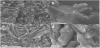
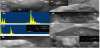
Figure 3 shows the TEM results for (Bi0.16Sb84)2Te3 sliced normal (Figure 3 (a-c)) and parallel (Figure 3(d-h)) to the pressing direction. The low magnification TEM image for (Bi0.16Sb84)2Te3 sliced normal to the pressing direction (Figure 3(a)) demonstrates that many nanoparticles with size of 50-80nm existed in the matrix with submicron size in three forms: along grain boundaries, inside grains and filling the pores. The typical HRTEM image (Figure 3(b)) of an individual nanoparticle reveals that the products are well crystallized and the lattice fringes can be observed clearly. The regular parallel fringe spacing is about 6.44 Å and 3.93 Å, which can be assigned to the interplanar spacing of the (11 1) and (2 2 0) lattice plane of cubic Sb2O3. The Fourier transfer diffraction pattern of white square part for nanoparticle is given in the inset of Figure 3(b), confirming that the nanoparticle is Sb2O3.The energy dispersive X-ray spectroscopic (EDX) patterns (Figure 3(c)) obtained on the nanoparticle confirm that they are compound of element Sb and O with the atomic ratio of Sb : O=2 : 2.95. As indicated in the low magnification TEM image of Figure 3(d) for (Bi0.16Sb84)2Te3 sliced parallel to the pressing direction, the dark triangle submicron particles are observed to exist along the grain boundaries, and the bright nanoparticles with size of around 50nm in the pore are found in the matrix. The EDX analysis for the dark triangle particle as shown in Figure 3(e) indicates that it is Tellurium. The selected-area electron diffraction (SAED) image taken from the dark triangle particle in theinset of Figure 3(e) confirms that it is a well-crystallized Te crystal. An amplified HRTEM image focusing on theedge of Te particle is presented in Figure 3(f), which indicates that the lattice spacing of about 5.96Å corresponds to (001) planes ofhexagonal Te. The HRTEM image of bright nanoparticle as shown in Figure 3(g) reveals that the interplanar spacing of about 6.44 Å can be assigned to the (11 1) lattice plane of cubic Sb2O3. The amplified HRTEM image for matrix is presented in Figure 3(h). The lattice spacing of about 1.02nm corresponds to (0 0 3) planes of rhombohedral (Bi0.16Sb84)2Te3. SAED image taken from the matrix in theinset of Figure 3(h)shows that spacing distance of 1.02nm is a five-layer lamellae with orientation arrangement along the [0 0 1] direction. EDX results obtained on the matrix indicate that the atomic ratio for Bi: Sb:Te in (Bi0.16Sb84)2Te3 is 0.34:1.59:3.
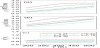
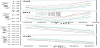
Temperature dependence of electrical resistivity measured
normal
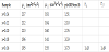
The Hall coefficient, RH, at room temperature (RT) is positive for
(BixSb1-x)2Te3 (0.16≤x≤0.24), indicating p-type or hole conduction
in this system, which agrees with the results of Seebeck coefficient.
Assuming parabolic bands and a single band conduction process at
300 K, the carrier concentration, p, is estimated from the formula:
p=1/eRH, where e is the carrier charge. The carrier concentrations
p are 1.54×10¹⁹, 2.10×10¹⁹, 2.76×10¹⁹, 3.33×10¹⁹ and 3.73×10¹⁹
cm-3 for samples with x=0.24, 0.22, 0.20, 0.18 and 0.16, respectively
(Table 2). Hence, it is the increase incarrier concentration that causes
the decrease in electrical resistivity with decreasing bismuth content.
The RThole mobilityis calculated from the equation μ=1/(ρpe), andis
listed in Table 2. One can see that for the same sample
which tells us that S decreases with increasing p,
η is the reduced Fermi energy, Fn(η) is the nth order Fermi integral,
h is Plank constant, kB is the Boltzmann constant, and r is scattering
parameter of relaxation time. In our calculations, we assume acoustic
phonon scattering dominates (i.e., r=-1/2), and the effective mass md*
is obtained to be 1.01m0 (where m0 is the free electron mass) for S0,
which is close to the reported value of m0 [15]. Assuming md* for the
nano-composite samples is the same as that of S0 and does not change
in different samples,
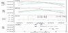
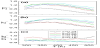
The effects of temperature on the thermal conductivity (
Where
Obviously in this case,
Subtracting the carrier thermal conductivity (κC), expressed as
κC=L0T/ρ (here L0 is the Lorenz number (2.0 × 10⁻⁸V2K-2) and ρ is the
electrical resistivity [15,17], from κ, the lattice thermal conductivityin
the direction normal
The reduction of
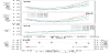
The calculated power factor (
4. Conclusions
(BixSb1-x)2Te3 (0.16≤x≤0.24)bulk samples are prepared by the melting
method, mortar type grinding and spark plasma sintering technique.
Due to the isotropic microstructure, highly isotropic resistivity
Competing Interests
The author declare that there is no competing interests regarding the publication of this article.
Author Contributions
All the authors substantially contributed to the study conception, the acquisition of results, and the interpretations as well as drafting the manuscript.
Acknowledgments
We greatly thank X. G. Zhu for his help in the analysis of TEM.