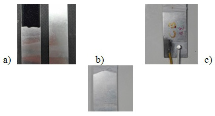
Figure 1:
(a) CNTS coated (left) and anodized (anodized) substrates, (b) the back side with the copper wire and AE sensor on the left and right respectively, and c) front side of the specimens.